What Is PCB Design and How Does It Work?
A printed circuit board turns an electrical concept into a physical system of copper paths, insulating layers, and carefully placed components. PCB design is the process of defining that system so signals, power, heat, and mechanical constraints work together. It is more than drawing traces. A designer must also consider component footprints, layer stack-up, spacing, manufacturing limits, and how the finished board will be assembled and tested.
The market context makes these decisions consequential. Prismark’s 2024 industry report estimated global PCB production value at about $69.5 billion in 2023. It also reported an approximately 15% year-over-year decline, highlighting how demand can shift across the electronics supply chain. These figures describe an industry, not the success of any individual design. Still, they underline why reliable engineering and manufacturable layouts matter. A board that looks correct on screen may fail when a connector footprint is wrong or a high-speed trace crosses a noisy region.
This guide explains how PCB design works, from requirements and schematics to layout, review, and fabrication files. It also shows how design choices affect performance, cost, and production readiness. Small details matter. A little humility matters, too: design rules reduce risk, but they do not replace prototype testing or feedback from the manufacturer.
What PCB Design Is and What It Defines
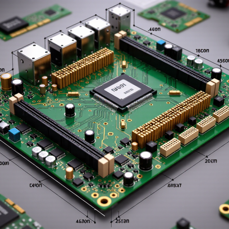
PCB design turns an electrical idea into a physical board that can be manufactured and assembled. It defines where components sit and how copper traces connect their pins. A schematic describes the intended connections; the board layout gives those connections real positions and dimensions. It also specifies the board outline, layer arrangement, copper thickness, holes, and spacing between features.
These choices affect more than appearance. Trace width and routing influence current capacity and signal behavior. Component spacing affects heat flow and whether parts can be soldered or inspected. Layer count and material influence cost and performance. The design files also communicate manufacturing details, such as drill locations and copper patterns. A layout can look tidy on screen yet be awkward to assemble; that gap is easy to underestimate.
Tips: Check footprints against component datasheets, not just library labels. Review clearances and board edges before sending files for fabrication. Ask for a second review, too. A small footprint mismatch can create a surprisingly expensive rework.
How Circuit Requirements Are Translated into a Schematic
What Is PCB Design and How Does It Work?
How Circuit Requirements Are Translated into a Schematic
A schematic turns a circuit’s required behavior into a clear map of electrical connections. Before drawing, define what the device must do, its supply voltage, expected current, inputs, outputs, and operating conditions. These details shape component choices and connection rules. For example, a temperature sensor may need a stable supply, a signal path to a processor, and filtering to reduce electrical noise. Write down these needs, even when some values are estimates. Assumptions can change.
Next, place symbols for the components and connect them with labeled nets. A power symbol, ground connection, resistor, and sensor should each represent a real electrical role, not merely fill space. Add values and part identifiers so another engineer can review the design without guessing. Keep related functions together. Small details matter. A connector’s pin order, for instance, can affect how a cable meets the board.
Check current paths, voltage limits, and unused pins against component documentation. Then run electrical checks to flag open connections or conflicting outputs. Such checks catch common mistakes, but they cannot confirm every design choice. A schematic may look tidy and still miss a real operating condition. Review it against the original requirements, and revise uncertain points before creating the board layout.
How Components and Copper Traces Are Arranged on the Board
PCB design decides where components sit and how copper connects them. Placement usually follows the circuit’s signal flow: connectors near board edges, processing parts grouped by function, and power components kept near their loads. Decoupling capacitors belong close to the relevant power pins, with short connections to ground. Short paths matter. They reduce unwanted resistance and inductance, though exact results depend on frequency and current. A tidy layout can still fail electrically; appearance is only a weak guide.
Copper traces carry signals and power, while planes provide return paths and help spread heat. Designers choose trace width according to current, copper thickness, and temperature rise. High-speed differential pairs need controlled spacing and consistent routing, not just matching lengths. Avoid splitting a ground plane beneath fast signals, because return current may take a longer, noisier route. Grand View Research estimated the global PCB market at $76.12 billion in 2023, underscoring how widely these design choices matter across electronics. That market figure does not measure design quality, of course. Layout software can flag rule violations, but physical review still matters: a connector may block assembly access, or a trace may crowd a mounting hole. Real boards often expose one overlooked detail.
How PCB Layouts Are Checked and Refined
What Is PCB Design and How Does It Work?
How PCB Layouts Are Checked and Refined
A PCB layout is more than a neat map of copper. It must connect components while meeting electrical, mechanical, and manufacturing limits. Review begins with design-rule checks, which flag issues such as insufficient spacing, narrow traces, and missing connections. Engineers then inspect the board in 3D, checking connector access, component height, and whether heat-sensitive parts sit too close to hot components. IPC-2221 provides widely used guidance for board design, but project-specific requirements still matter. A rule pass does not guarantee a reliable board.
The next stage combines signal-integrity analysis, thermal checks, and design-for-manufacturing review. Engineers may adjust trace widths, add ground vias, or shift a component by a few millimeters to reduce noise or ease assembly. Small errors matter. A 2020 peer-reviewed PCB inspection study introduced the DeepPCB dataset, containing 1,500 image pairs across six defect types. That figure shows why automated inspection can help, but it does not replace expert review: image-based checks cannot judge every electrical or mechanical risk. Not perfect. Teams should compare analysis results with prototype measurements, then revise the layout when real behavior differs from simulation. Sometimes, a late change fixes one problem and creates another. That trade-off deserves another review.
How Design Files Guide PCB Fabrication and Assembly
A PCB design file is a manufacturing instruction set, not just a picture of a circuit. It defines copper layers, drill locations, solder-mask openings, component positions, and board thickness. Fabricators use these details to make the bare board. Assembly teams use the bill of materials and placement data to fit parts accurately.
Small mismatches matter.
A drill file that does not match the layer data can shift a via or leave a component pad unusable.
The handoff usually includes layer images, drill files, a board outline, a stack-up, and assembly documents. IPC-2581 provides a standardized way to package several manufacturing and assembly data types together.
IPC’s 2023 PCB Technology Trends Study identifies higher density, faster signaling, and finer features as ongoing design pressures. Those pressures make clear, consistent files more important: a missing impedance note can affect signal performance, while an outdated parts list can stall assembly.
Still, a tidy package is not proof of a correct board. Engineers should compare the exported files with the final design and review manufacturing feedback. I have seen one overlooked note create avoidable back-and-forth. It is easy to miss.