
What Are the Top Types of PCB Board Design?
Choosing the right pcb board design begins with the product’s electrical, mechanical, and manufacturing demands. A simple sensor may need a single-sided board. A compact industrial controller often requires a double-sided or multilayer structure. Wearable devices may depend on rigid-flex construction, while dense smartphones commonly use HDI technology.
“No single ranking is perfect.” The best option depends on signal speed, component density, thermal load, budget, and assembly limits. Signal integrity expert Howard Johnson famously stated, “It is not the clock frequency that determines whether a circuit is high speed, it is the rise time.” This principle remains practical. A fast edge can create noise across a short copper trace.
A reliable pcb board design also considers trace width, impedance control, return paths, via placement, and grounding. For example, a four-layer board can place power and ground planes close together. That arrangement shortens return paths and reduces electromagnetic interference. Flex sections need controlled bend radii, not sharp folds beside solder joints.
Manufacturers and engineers often review designs against IPC guidance, fabrication tolerances, and thermal requirements. Yet standards do not replace judgment. A technically correct layout can still fail after repeated bending, poor connector placement, or unexpected heat buildup. That is the uncomfortable part.
This overview compares the leading PCB types and explains where each structure performs best. It also examines trade-offs that are easy to overlook, including cost, repairability, production volume, and long-term reliability. The “best” board is rarely the most advanced one. It is the one that fits the real product.
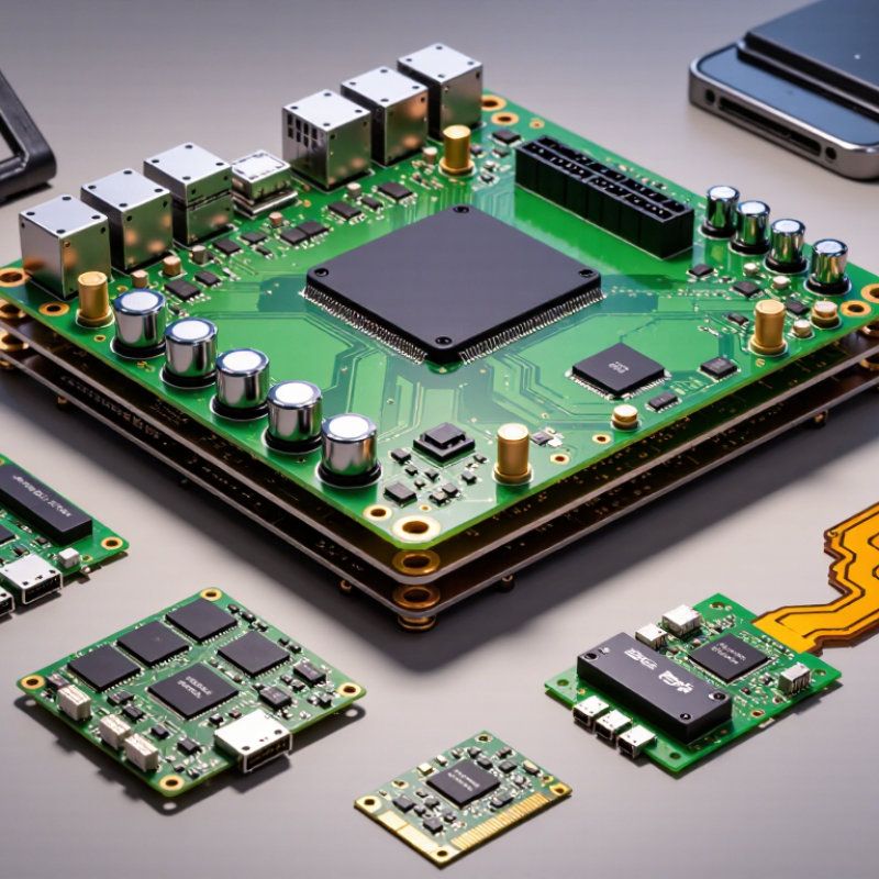
Single- and Double-Sided PCBs: 1–2 Copper Layers Under IPC-2221
Single- and double-sided boards use one or two copper layers, respectively. They are common choices for simple circuits and compact products. IPC-2221 offers generic guidance for PCB design, but it does not prescribe one universal layout or trace width. Designers must consider current, voltage, copper thickness, materials, and manufacturing capability.
On a single-sided board, components and copper traces usually occupy opposite faces. This keeps construction straightforward, but routes can quickly run out of room. A crossing may require a jumper wire or a changed component position. That simplicity has a cost. For a small sensor board, even moving one connector can open a cleaner path between components.
A double-sided board adds copper on the opposite face. Traces can pass beneath components or cross other routes by changing layers. Plated through-holes and vias connect the copper layers, so their placement matters. Keep enough clearance around pads and holes, and check that narrow traces can carry the expected current. IPC-2221 helps frame those decisions; it is not a substitute for checking the board fabricator’s tolerances. I would also review the routing after the first layout. A design may meet basic spacing needs yet still be awkward to assemble or inspect.
Multilayer PCB Design: Four or More Copper Layers and Sequential Build-Up
A multilayer PCB has four or more copper layers, pressed together with insulating material. Designers use inner layers for power planes, ground returns, or dense signal routing. This can shorten connections and reduce interference, but it makes the stack-up less forgiving. A misplaced via may cross several layers before reaching its destination. Small errors travel.
Not every four-layer board needs sequential build-up. That process adds and laminates layers in stages, often enabling fine-pitch routing and microvias in high-density designs. Each extra build-up cycle adds alignment, drilling, and inspection demands. Prismark’s 2024 industry analysis estimated global PCB production value at about US$73.4 billion in 2023. The figure covers the wider PCB sector, not multilayer boards alone, so it should not be read as a measure of multilayer demand. In practice, engineers should define layer count from routing, impedance, thermal, and manufacturing needs—not from density targets alone. A six-layer design may solve a real routing problem; sometimes it only adds cost. That distinction is easy to miss.
HDI PCB Design: Microvias and Fine Features Defined by IPC-2226
HDI PCB design is defined by controlled miniaturization, not simply smaller traces. IPC-2226 describes microvias as small, usually laser-formed structures with limited depth and controlled aspect ratios. A practical microvia often measures 150 micrometres or less in diameter. Its short vertical path reduces routing distance between adjacent layers. That matters in compact processors, cameras, and wearable devices.
Industry data shows why this technology keeps expanding. A 2024 global PCB market report estimated HDI boards would grow at about 6% annually through 2030. The same report linked growth to smartphones, automotive electronics, and high-density computing. IPC’s 2023 technology roadmap also identifies fine-line routing and sequential build-up structures as major manufacturing priorities. Yet tiny features create large consequences. A slight drill offset can reduce the capture pad margin. Resin voids may remain invisible until thermal cycling.
Designers should set fabrication rules before routing begins. Common HDI layouts use 75–100 micrometre trace and space values, but capability varies by fabricator. IPC-2226 provides guidance, not a substitute for process validation. Stackup trials, cross-sections, and thermal cycling reveal weaknesses early. I have seen dense layouts fail because engineers optimized routing first and reviewed escape geometry later. That approach is efficient only on paper. Reliable HDI design needs realistic tolerances, filled or capped microvias where required, and inspection data tied to each critical layer.
| PCB Design Type | Typical Construction | Typical Feature Capability | Via Technology and HDI Classification | Common Applications | Primary Benefits and Limitations |
|---|---|---|---|---|---|
|
Basic Single-Sided PCB |
One conductive copper layer on one side of an insulating substrate; components and solder joints are generally placed on the same side. | Usually uses relatively large pads, tracks, and through-holes. Routing density is low compared with multilayer and HDI designs. | Through-holes may be used, but blind, buried, and microvia structures are normally unnecessary. | Simple controls, low-density power circuits, basic consumer devices, and cost-sensitive electronic assemblies. | Lowest manufacturing complexity and cost, but limited routing space, weak support for dense interconnects, and less flexibility for high-speed signal separation. |
|
General Purpose Double-Sided PCB |
Copper layers on both sides of the dielectric substrate, connected by plated through-holes. | Higher routing capacity than a single-sided board; typical designs use conventional line widths and spaces selected for standard fabrication capability. | Primarily plated through-holes. Blind and buried vias can be added in advanced constructions but are not inherent to the format. | Industrial controls, lighting, instrumentation, power supplies, and moderate-complexity embedded electronics. | Good balance of cost and capability; routing can become difficult when component count, signal speed, or power-distribution requirements increase. |
|
High Density Conventional Multilayer PCB |
Three or more copper layers separated by dielectric materials, commonly including dedicated power and ground planes. | Increased wiring density, controlled impedance capability, improved power distribution, and better electromagnetic compatibility than simpler board types. | Plated through-holes are common. Some designs use blind or buried vias, but standard multilayer construction does not necessarily qualify as HDI. | Computers, networking equipment, industrial controllers, automotive electronics, medical instruments, and communication systems. | Supports complex routing and signal integrity, but increases layer-registration requirements, material consumption, fabrication time, and inspection demands. |
|
Flexible Flex and Rigid-Flex PCB |
Flexible polyimide-based sections, or a combination of rigid laminate areas and flex interconnect sections. | Feature sizes depend strongly on bend radius, dynamic-flex requirements, copper type, and the number of flex layers. | Plated through-holes, blind vias, and microvias may be used. Microvias can help reduce bending-area congestion when properly placed. | Wearable devices, cameras, compact displays, medical instruments, aerospace electronics, and products requiring folding or three-dimensional assembly. | Reduces connectors and assembly space and permits mechanical movement; requires careful control of bend radius, copper fatigue, coverlay design, and material transitions. |
|
HDI IPC-2226 Type I |
A conventional core with one microvia build-up layer on one or both sides, combined with through-hole interconnections. | Fine lines and spaces are commonly designed around approximately 75–100 µm in advanced fabrication, although the allowable value is process-dependent. | Laser-drilled microvias connect adjacent layers. Type I generally uses microvias and through-holes without a required buried-via layer. | Compact digital products, dense component areas, small modules, and designs where a modest increase in routing density is needed. | Improves escape routing and component placement density with less layer growth; requires laser drilling, controlled dielectric thickness, and strict registration control. |
|
HDI IPC-2226 Type II |
A multilayer core incorporating buried vias, with one microvia build-up layer on one or both outer sides. | Supports fine-pitch breakout and additional internal routing. Typical microvia finished diameters are about 50–150 µm, subject to manufacturing capability. | Uses microvias, through-holes, and buried vias. Microvias normally connect adjacent layers and are commonly formed by laser drilling. | High-density computing, communications, instrumentation, and compact control electronics. | Offers more routing flexibility than Type I; buried-via fabrication adds process steps, registration challenges, material usage, and inspection requirements. |
|
HDI IPC-2226 Type III |
A multilayer core with two or more microvia build-up layers on one or both sides, generally combined with through-holes and possibly buried vias. | Designed for very dense escape routing, fine-pitch packages, and high layer-to-layer interconnect density. Microvia aspect ratio is commonly designed near 1:1. | Uses multiple microvia layers, through-holes, and buried vias. Stacked or staggered microvias may be selected according to reliability and process requirements. | Advanced mobile electronics, high-performance computing modules, compact communication hardware, and highly integrated embedded systems. | Maximizes routing density and can reduce overall board size; has the highest sensitivity to lamination, registration, via reliability, thermal stress, and process variation among these HDI types. |
|
Advanced HDI Any HDI Type with Stacked Microvias |
Two or more microvias are vertically aligned and connected through successive dielectric layers; copper filling may be used to support reliable stacking. | Enables dense vertical interconnection beneath fine-pitch components and can reduce via keep-out area compared with fully staggered structures. | Stacked microvias are associated with advanced HDI implementation rather than a separate universal IPC-2226 type. The design must define stack height, fill method, and reliability controls. | Very compact packages, high-I/O devices, miniaturized modules, and boards requiring maximum escape-routing efficiency. | Provides exceptional density and compactness; increases manufacturing complexity, copper-fill requirements, thermal-mechanical stress, and the need for qualification testing. |
Flexible PCB Design: Bendable Circuits Governed by IPC-2223
What Are the Top Types of PCB Board Design?
Flexible PCB design uses bendable copper circuits on polymer films. IPC-2223C provides the main design framework for these structures. It addresses bend zones, coverlay, stiffeners, conductor spacing, and mechanical stress. The standard is useful, but it cannot replace physical testing.
WSTS forecast global semiconductor sales at 611 billion dollars in 2024, representing 16% growth. That expansion increases pressure for compact, lightweight electronics and more flexible interconnects. In practice, designers must separate static bends from repeated dynamic bends. A cable folded once needs a different structure from a hinge cable moving thousands of times.
Keep copper traces away from the neutral axis when repeated flexing is expected. Avoid sharp corners near the bend area. Rounded routing helps reduce stress concentration. A typical prototype may use a 0.5-millimeter bend radius, but the correct value depends on layer count, copper thickness, and material behavior.
Small details matter. A stiffener should end outside the active bend zone. Vias also deserve caution because their barrels can become mechanical stress points. IPC-2223C offers guidance, yet real assemblies may behave differently after heat, vibration, and repeated motion. A bend test can pass while the final enclosure still causes failure. That is where my confidence becomes limited. Mechanical trials remain essential.
What Are the Top Types of PCB Board Design?
Flexible PCB Design: Bendable Circuits Governed by IPC-2223
The chart presents commonly used minimum bend-radius starting points as multiples of the finished flex-circuit thickness. Single-sided flex circuits generally allow tighter bends, while double-sided, multilayer, and rigid-flex constructions require progressively larger radii. IPC-2223 provides design guidance, but the final bend radius must be verified against the actual stack-up, copper pattern, materials, bend direction, and mechanical life requirements.
Rigid-Flex PCB Design: Combined Rigid and Flexible Structures Under IPC-6013
Rigid-flex PCB design combines rigid sections for component mounting with flexible sections for controlled movement. It can reduce connectors, save space, and simplify assembly.
Under IPC-6013, the design should address material selection, fabrication quality, and performance requirements for flexible and rigid-flex boards. In practice, bend zones need careful planning. Keep vias and large pads away from repeated bending areas. Define the bend radius from the stack-up, copper thickness, and flex construction. A sharp fold may pass a basic fit check, then fail after repeated movement.
Layer transitions deserve attention. Gradual transitions reduce mechanical stress between rigid and flexible regions. Stiffeners can support connectors, but they also increase local thickness. Coverlay openings must match pad geometry without exposing unnecessary copper. Copper balancing helps limit warpage during manufacturing.
Keep it practical.
A first layout rarely survives review unchanged. That is normal. Mechanical clearance, heat, and assembly access often reveal problems late. I have found that a simple bend-zone drawing prevents more confusion than a crowded three-dimensional model. Designers should document bend radius, flex length, stiffener locations, and inspection points. IPC-6013 supports a reliable quality framework, but it cannot replace communication between design and fabrication teams. Small assumptions still need verification.
Related Posts
-
Top PCB Printing Manufacturers for Global Buyers
-

Best PCB Prototype Solutions for Global Buyers Today?
-
Top 10 Types of PCB Design Global Buyers Need to Know
-

2026 How to Choose Circuit Board Manufacturing for Your Needs?
-
What Is PCB Manufacturing and Assembly?
-
How to Source Circuit Boards Efficiently in 2026?