Unlocking Efficiency: The Future of PCB Production Techniques in Modern Electronics
In the ever-evolving landscape of modern electronics, the quest for
enhanced efficiency in PCB production has never been more critical. As technology continues to advance, manufacturers are constantly seeking innovative techniques that streamline processes, reduce costs, and improve overall product quality. This dynamic environment presents a unique opportunity to explore "how to" optimize PCB production through the implementation of cutting-edge technologies such as additive manufacturing, automated workflows, and smart materials. By unlocking the potential of these innovative approaches, companies can not only enhance their production capabilities but also stay competitive in an increasingly complex market. In this guide, we will delve into various strategies and best practices that can transform PCB production, setting the stage for a future marked by greater efficiency and sustainability in the electronics industry.
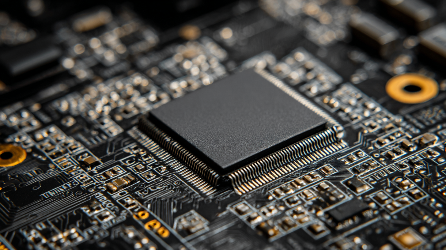
Exploring Advanced Manufacturing Methods for PCB Production
In the rapidly evolving landscape of modern electronics, the efficiency of PCB (Printed Circuit Board) production is paramount. Advanced manufacturing techniques are essential for keeping pace with the escalating demands for higher performance, reduced costs, and faster time-to-market. Recent data from the IPC (Association Connecting Electronics Industries) indicates that the global PCB market is anticipated to reach $82 billion by 2025, driven by the increasing miniaturization of devices and the surge in IoT and automotive applications. As a result, companies are increasingly turning to sophisticated manufacturing methods such as additive manufacturing (3D printing) and automated assembly processes to enhance production capabilities.
One of the most promising advancements is the implementation of Industry 4.0 principles in PCB production. According to a report by Mordor Intelligence, the smart manufacturing market is expected to grow from $190 billion in 2020 to over $520 billion by 2026. This shift enables real-time monitoring and optimization of production lines, reducing error rates and improving yield. Techniques such as laser direct imaging and advanced robotic assembly are not only streamlining workflows but also offering unprecedented flexibility to accommodate a variety of design specifications. As manufacturers adopt these innovative methods, they position themselves at the forefront of an industry that is increasingly defined by speed, precision, and adaptability.
Implementing Automation to Streamline PCB Assembly Processes
The electronics industry is witnessing a transformative shift as automation becomes integral to PCB assembly processes. According to a report by IPC, the adoption of automated systems in PCB manufacturing is projected to improve production efficiency by up to 30% within the next five years. Automation not only accelerates the assembly line but also enhances precision, which is crucial as the miniaturization of components continues to challenge traditional manufacturing techniques. By implementing state-of-the-art robotics and AI-driven machinery, companies can reduce human error and throughput times, meeting the escalating demand for complex electronic devices.
Moreover, the integration of automation technologies is leading to significant cost reductions. A recent study by MarketsandMarkets estimates that automated PCB assembly could lower labor costs by as much as 20%. This allows manufacturers to allocate resources more effectively while maintaining competitive pricing in a market increasingly influenced by rapid technological advancements and consumer expectations. The move towards automated setups ensures that businesses can not only keep pace with innovation but also provide higher quality products with greater reliability, setting the stage for a more efficient future in electronics production.
Unlocking Efficiency: The Future of PCB Production Techniques in Modern Electronics - Implementing Automation to Streamline PCB Assembly Processes
| Production Technique |
Automation Level |
Process Efficiency (%) |
Cost Reduction (%) |
Lead Time Reduction (Days) |
| Surface Mount Technology (SMT) |
High |
30 |
25 |
3 |
| Through-Hole Technology (THT) |
Medium |
20 |
15 |
5 |
| Automated Optical Inspection (AOI) |
High |
40 |
30 |
2 |
| Robotic Arm Assembly |
Very High |
50 |
35 |
1 |
| Selective Soldering |
Medium |
25 |
20 |
4 |
Adopting Eco-Friendly Materials in PCB Fabrication Techniques
The use of eco-friendly materials in PCB fabrication techniques is becoming increasingly important in the electronics industry, driven by both regulatory pressures and a growing awareness of environmental sustainability. According to a report from MarketsandMarkets, the eco-friendly PCB market is projected to reach $5.6 billion by 2025, growing at a CAGR of 8.9% from 2020. This shift towards greener materials not only reduces the environmental impact associated with traditional PCB production but also appeals to consumers increasingly interested in sustainable products.
One notable advancement is the innovation of biodegradable substrates and lead-free solder materials, which are gaining traction among manufacturers. A study from IPC estimates that nearly 30% of PCBs are now being produced with environmentally friendly processes, showcasing the industry's commitment to sustainability. Furthermore, the adoption of recycled materials in PCB fabrication indicates a shift towards a circular economy, reducing waste and resource consumption. As these practices become more prevalent, we can expect a significant transformation in the way PCBs are produced, ultimately leading to more sustainable electronic devices.
Leveraging AI and Machine Learning to Enhance PCB Design Efficiency
The integration of artificial intelligence (AI) and machine learning (ML) into PCB design processes is revolutionizing the electronics industry by enhancing efficiency and precision. By analyzing vast datasets, AI algorithms can identify patterns and predict design outcomes, leading to quicker iterations and a reduction in human error.
 This capability allows engineers to focus on more strategic design elements, while AI handles routine tasks such as component placement and signal integrity analysis. As a result, companies can significantly shorten their development cycles, enabling faster time-to-market for new products.
Moreover, machine learning models can continuously improve PCB designs by learning from previous iterations. With each new project, these models can adapt and suggest design modifications based on historical performance data. This iterative feedback loop not only enhances the quality of the designs but also fosters innovation, as designers are empowered to experiment with new configurations and technologies without the fear of detrimental mistakes.
Emphasizing the synergy between human creativity and AI-driven analytics, the future of PCB production looks bright, characterized by streamlined workflows and unparalleled design sophistication.
Integrating IoT Solutions for Real-Time Monitoring in PCB Production
In the rapidly evolving landscape of electronics, integrating IoT solutions for real-time monitoring in PCB production stands out as a major innovation. This approach not only enhances efficiency but also improves the precision of manufacturing processes. By employing IoT technologies, manufacturers can gather data from various stages of production, enabling them to monitor performance metrics and respond to anomalies instantaneously. This can lead to reduced downtime, minimized waste, and increased overall output.
Tips for implementing IoT in PCB production include starting small by pilot testing on specific machines to identify which processes benefit most from monitoring. It’s also crucial to ensure that the data collected is analyzed effectively, using advanced algorithms to predict potential failures before they occur. Additionally, fostering a culture of continuous improvement can empower employees to leverage these new technologies effectively.
As the optical particle counter market grows significantly, with projections suggesting a rise from $105.31 million in 2025 to $626 million by 2033, the PCB industry must acknowledge the implications of such advancements. Utilizing real-time monitoring can set manufacturers ahead of the competition, ensuring they remain agile in a market that demands both innovation and reliability.
Unlocking Efficiency: PCB Production Techniques