What Is Printed Circuit Board Assembly and How Does It Work?
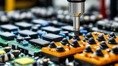
A printed circuit board assembly (PCBA) turns a bare board into a working electronic unit. It combines the board, electronic components, solder, and a controlled manufacturing process. The result may be a compact sensor, a laptop motherboard, or a controller inside industrial equipment. Each component must sit in the correct position and connect to the intended circuit.
IPC president and CEO John W. Mitchell is a recognized voice in electronics manufacturing. In paraphrase, his industry message is that reliable products depend on consistent manufacturing practices—not inspection alone. This is a paraphrase, not a verified verbatim quotation. That distinction matters when technical claims need to be traceable.
The process usually begins with solder paste applied through a stencil onto precise pads. A placement machine then sets components onto the board, sometimes handling thousands of tiny parts. The board passes through a reflow oven, where controlled heat melts the solder and forms electrical joints. Larger connectors or specialized components may need separate soldering steps. Small defects matter. A shifted resistor or a weak joint can interrupt a signal, cause heat buildup, or shorten product life. Automated optical inspection and electrical tests help catch problems, but no single check proves every assembly will perform perfectly in every environment.
Understanding printed circuit board assembly means looking beyond the machines. Design choices, component quality, process settings, and testing all shape the outcome. Factory conditions differ, and this overview cannot cover every assembly method. That limitation deserves attention. A useful guide should explain the typical workflow while making clear where real production decisions require expert judgment.
What Printed Circuit Board Assembly Means
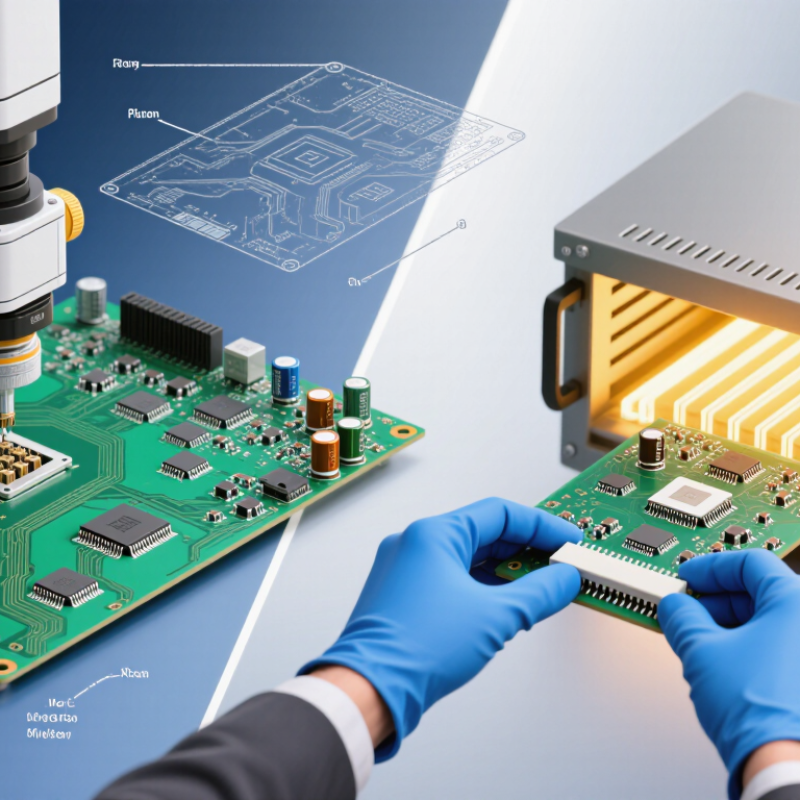
Printed circuit board assembly, or PCBA, means a bare circuit board populated with electronic components and joined into a working electronic unit. The board provides conductive paths; components such as resistors, chips, and connectors perform specific functions. Assembly usually includes applying solder paste, placing surface-mount parts, heating the board, and inspecting solder joints. Through-hole components may also be inserted and soldered. The result is not merely a board with parts attached. It is an interconnected circuit built to meet a design’s electrical and physical requirements.
The distinction matters. A printed circuit board, or PCB, is the unpopulated foundation; a PCBA is that foundation after components are mounted. Fortune Business Insights estimated the global PCB market at USD 81.45 billion in 2023. That figure covers boards, not assembly alone, but it shows the scale of the hardware ecosystem behind PCBA work. In practice, assembly quality depends on details: a misplaced chip, insufficient solder, or heat-sensitive component can affect performance. Automated inspection helps identify visible defects, though it cannot prove every circuit works as intended.
Assembly choices depend on the product. A compact sensor may use mostly surface-mount parts, while a power device may need larger through-hole components. Design files, component tolerances, and test requirements all shape the process. The boundary between “assembly” and “manufacturing” is not always perfectly neat; different suppliers may use the terms differently. A useful specification therefore states what is included, such as component placement, soldering, inspection, and functional testing.
The Components and Materials Used in PCBA
A PCBA begins with a bare printed circuit board, which supports components and connects them through copper paths. Many boards use FR-4, a rigid material made from woven glass fibers and epoxy resin. Flexible designs may use other substrates. Copper layers carry electrical signals, while the solder mask protects copper from oxidation and helps prevent accidental solder bridges. The small printed labels identify component locations. They are useful, though crowded boards can make them hard to read.
Components give the board its working functions. Resistors limit current, capacitors store and release charge, and diodes guide current in one direction. Integrated circuits handle tasks such as processing signals or controlling power. Connectors link the assembly to cables, sensors, or other boards. Component choice depends on voltage, heat, space, and the operating environment. A part that fits the footprint may still be unsuitable if it overheats.
Solder paste, typically a blend of tiny metal particles and flux, holds components in place before heating. During reflow, the metal melts and forms electrical and mechanical joints. The board’s surface finish helps those joints form reliably. Small details matter. Uneven paste or a poorly aligned component can cause defects that are difficult to spot by eye. Material choices also involve trade-offs: a lower-cost substrate may work well in one device, but not under repeated heat or vibration. There is no single ideal combination for every assembly.
| Category | Component or Material | Typical Material or Construction | Purpose in the Assembly | How It Is Used in PCBA |
|---|---|---|---|---|
| Printed circuit board | Substrate | Often woven glass fiber reinforced with epoxy resin, commonly called FR-4 | Provides mechanical support and electrical insulation for the circuit. | Components are mounted on the board, while copper tracks route electrical signals and power. |
| Printed circuit board | Copper layers and pads | Patterned copper foil; multilayer boards use copper layers separated by insulating material | Forms conductive paths, component pads, and connections between layers. | Components are soldered to exposed pads; plated vias can connect copper layers. |
| Printed circuit board | Solder mask | Protective polymer coating applied over much of the copper | Helps prevent solder bridges and protects copper from contamination and oxidation. | Openings in the coating expose pads and other areas that need soldering. |
| Printed circuit board | Surface finish | Examples include immersion tin, immersion silver, and electroless nickel immersion gold (ENIG) | Protects exposed copper pads and supports solderability. | The finish is applied to exposed copper areas before components are assembled. |
| Electronic component | Resistor | Common surface-mount types use a ceramic body with resistive material and metal terminations | Limits current, divides voltage, or sets operating conditions in a circuit. | Surface-mount resistors are commonly placed onto solder-pasted pads by automated equipment. |
| Electronic component | Capacitor | May use ceramic dielectric layers or an electrolytic construction, depending on type | Stores electrical charge and is used for filtering, decoupling, timing, and other functions. | Small surface-mount capacitors are commonly reflow-soldered; some larger types may be through-hole mounted. |
| Electronic component | Integrated circuit (IC) | Silicon semiconductor die enclosed in a package with conductive leads or terminals | Performs functions such as processing, memory, amplification, or power control. | Package terminals are soldered to matching board pads; package styles determine placement and soldering requirements. |
| Electronic component | Connector | Typically combines conductive metal-alloy contacts with an insulating polymer housing | Provides detachable electrical connections to cables, modules, or other boards. | May be surface-mount or through-hole mounted, depending on its design and mechanical requirements. |
| Assembly material | Solder paste | Fine solder-alloy powder mixed with flux; lead-free SAC305 is one commonly used alloy | Temporarily holds surface-mount components and forms electrical and mechanical joints when heated. | A stencil deposits paste onto surface-mount pads before components are placed and the board is heated. |
| Assembly material | Flux | Chemical activators and other ingredients formulated for the chosen soldering process | Removes or disrupts surface oxides and helps solder wet the metal surfaces. | Flux is included in solder paste or applied separately for processes such as wave soldering. |
| Assembly process | Solder paste printing and component placement | Stencil printer, solder paste, and automated pick-and-place equipment | Applies solder paste to intended pads and positions components accurately. | Placement follows the board design and assembly data; visual or automated checks can identify placement issues. |
| Assembly process | Reflow soldering | Controlled heating profile in a reflow oven | Melts solder paste to create joints between surface-mount terminals and board pads. | The board is heated through defined stages, then cooled; the profile is selected for the components and materials. |
| Assembly process | Through-hole soldering | Wave soldering, selective soldering, or manual soldering, depending on the assembly | Creates solder joints for component leads inserted through board holes. | Through-hole parts are inserted before solder is applied to the leads and plated holes. |
| Quality control | Inspection and testing | Visual inspection, automated optical inspection (AOI), in-circuit testing, or functional testing | Checks assembly quality and verifies electrical connections or product operation. | Methods are selected according to board complexity, production volume, and test requirements. |
How a Bare PCB Is Prepared for Assembly
A bare PCB is not ready for component placement just because its copper tracks look clean. Prismark’s 2024 industry review reported that global PCB production value rose 5.8% to about US$73.4 billion in 2024, reflecting the scale of boards moving through manufacturing. Preparation starts at receiving: technicians compare each panel with its drawing, checking dimensions, thickness, surface finish, solder mask, and visible damage. Automated optical inspection can reveal open circuits or shorts. Small defects matter. A warped panel, for example, may sit unevenly against assembly equipment.
The board is then cleaned only when the finish and process allow it; aggressive cleaning can damage surfaces. Moisture-sensitive boards may need controlled drying, but the correct conditions depend on material and supplier guidance. Technicians also confirm fiducial marks and tooling features, which help machines align the panel before solder paste printing and component placement. IPC-6012 provides qualification and performance requirements for rigid printed boards, while the assembly line uses its own documented acceptance checks. A practical gap remains: a board can pass visual inspection yet still have poor solderability, so process teams may verify finish condition before production. That check is easy to overlook.
How Components Are Mounted and Soldered
In printed circuit board assembly, components are placed onto a prepared bare board and electrically joined through solder. For surface-mount technology, solder paste is pressed through a stencil onto copper pads. A placement machine then sets tiny resistors, capacitors, and chips into the paste. Small parts matter. Even a slight shift can bridge adjacent pads or leave a weak connection.
The board passes through a reflow oven, where controlled heat melts the solder and forms joints. Temperature zones must suit the paste and component mix; excessive heat can damage parts, while insufficient heat may leave joints poorly formed.
Through-hole components follow a different route: leads pass through drilled holes, then wave or selective soldering joins them to pads underneath. IPC J-STD-001 sets requirements for soldered electrical assemblies, while IPC-A-610 guides visual acceptance.
Inspection may combine cameras, X-ray imaging, and electrical tests. Then comes inspection. It is easy to over-trust a clean image; hidden voids or poor wetting can still escape a quick visual check.
Fortune Business Insights’ PCB Market report valued the global PCB market at USD 81.25 billion in 2023, underscoring the scale of production where repeatable placement and solder control matter.
How the Assembled Board Is Inspected and Tested
After soldering, inspection begins with the board still warm from the reflow oven. Automated optical inspection checks component position, polarity, solder bridges, and visible joint shape. It is fast, but it cannot see hidden connections beneath many components. X-ray imaging can reveal voids or misaligned joints there; a technician may still need to interpret uncertain images.
Electrical testing adds another layer. In-circuit testing checks selected connections and components, while functional testing powers the board and checks its real behavior. IPC-A-610J provides workmanship acceptance criteria, and IPC-9252B addresses bare-board electrical testing. These standards guide decisions, but they do not make every defect detectable. No test is perfect. Test limits, fixture wear, and poorly chosen coverage can let faults escape. Teams should record test results, review recurring failures, and verify that test programs match the current design. That review is easy to neglect.
The waste stakes are tangible. The Global E-waste Monitor 2024 reports that the world generated 62 million tonnes of e-waste in 2022, with 22.3% documented as formally collected and recycled. That figure covers all e-waste, not PCBs alone, but it underscores why preventing avoidable scrap matters. A careful inspection plan cannot eliminate every failure. It can catch many problems before boards reach equipment or customers.
Related Posts
-
Why Choose PCB Assembly Services for Global Sourcing?
-
What Is PCB Manufacturing and Assembly?
-
What Is PCB Manufacturing and Assembly?
-
How to Choose a PCB Manufacturing and Assembly Partner?
-
Innovative Trends in PCB Printing That Will Transform the Electronics Industry
-

Top Circuit Board Manufacturing Trends at 2026 Canton Fair?