What is a PCB Maker and How Do They Work?
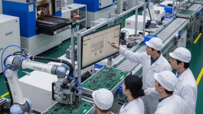
In the realm of electronics, a PCB maker is essential. They create printed circuit boards that form the backbone of countless devices. These boards connect different electronic components, enabling them to function together seamlessly.
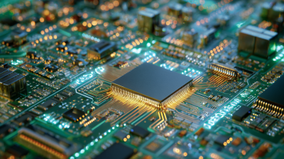
A PCB maker uses advanced technology to design and produce these crucial boards. The process begins with intricate design layouts. They convert these designs into physical boards through various manufacturing steps. This involves layering, etching, and sometimes soldering components onto the boards.
However, challenges persist in this field. Manufacturers often face issues with quality control and precision. Minor errors in design can lead to significant malfunctions. It is vital for a PCB maker to continually refine their processes. Their role is not just about production, but also ensuring reliability and performance of the final product.
What is a PCB Maker?
A PCB maker is a specialized manufacturer that produces printed circuit boards (PCBs). These boards are essential components found in electronic devices. They consist of insulating materials with conductive pathways for connections. The process involves designs that engineers create using CAD software. Understanding these designs is crucial for PCB makers.
In recent years, the global PCB market has seen significant growth. According to a report by Research and Markets, the market size is projected to reach over $70 billion by 2027. With increased demand for electronics, PCB makers face challenges. Quality control becomes critical. Many makers implement rigorous testing protocols. Mistakes can lead to failures in electronic devices, which can be costly.
Tips: Always clarify your design specifications before sending them to a PCB maker. Miscommunication can cause delays. Additionally, choose a maker with a solid reputation in the industry. This decision can save time and resources.
Attention to detail is vital in PCB manufacturing. Even small errors can lead to big problems. A successful PCB maker knows the importance of precision. They continuously invest in technology to enhance performance. The rapidly changing technology landscape pushes these makers to adapt. Staying updated is not just a choice; it’s a necessity.
What is a PCB Maker and How Do They Work?
| Parameter |
Description |
| Material |
Typically FR-4, CEM-1, or flexible materials. |
| Layer Count |
Single, double, or multi-layer designs. |
| Manufacturing Process |
Includes design, etching, drilling, plating, and lamination. |
| PCB Thickness |
Commonly ranges from 0.2 mm to 3.2 mm. |
| Surface Finish |
Options include HASL, OSP, ENIG, and immersion silver. |
| Lead Time |
Typically ranges from 3 days to several weeks depending on complexity. |
| Application |
Used in consumer electronics, automotive, industrial equipment, and medical devices. |
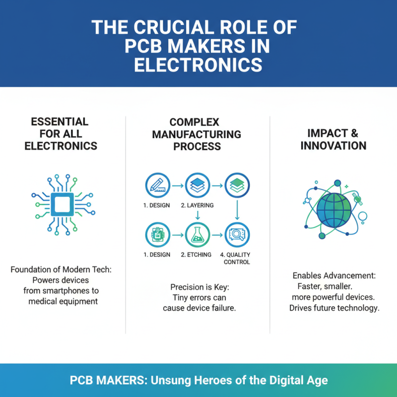
The Role and Importance of PCB Makers in Electronics
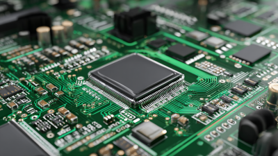
PCB makers play a crucial role in the electronics industry. They create printed circuit boards, which are essential for almost all electronic devices. Without them, modern technology would struggle to function efficiently. The process of making PCBs involves several steps, such as design, layering, and etching. Attention to detail is vital in each phase. Even a minor mistake can lead to device failure.
These makers ensure high precision and quality in their outputs. They work with various materials like copper and fiberglass. Each component must be perfectly aligned to avoid potential glitches. Engineers often rely on their expertise to bring designs to life. However, the industry faces challenges. Sometimes, delays occur due to material shortages or production errors. Continuous reflection on these issues is necessary for improvement.
Understanding the importance of PCB makers helps appreciate their contribution to technology. They enable innovations that shape our lives. Yet, there is always room for growth. Balancing efficiency with precision remains a constant struggle for many. The future demands better solutions, and PCB makers must adapt.
The PCB Manufacturing Process: Step-by-Step Overview
The PCB manufacturing process is intricate and multifaceted. It begins with design. Engineers create a layout using specialized software. This design must be precise. Any small error can lead to bigger issues later.
Next comes the production phase. Actual materials are chosen, such as copper and fiberglass. The layers are carefully prepared. Some manufacturers use automated machines, while others rely on manual processes. Each method has its strengths and weaknesses. However, manual methods might lead to inconsistent quality.
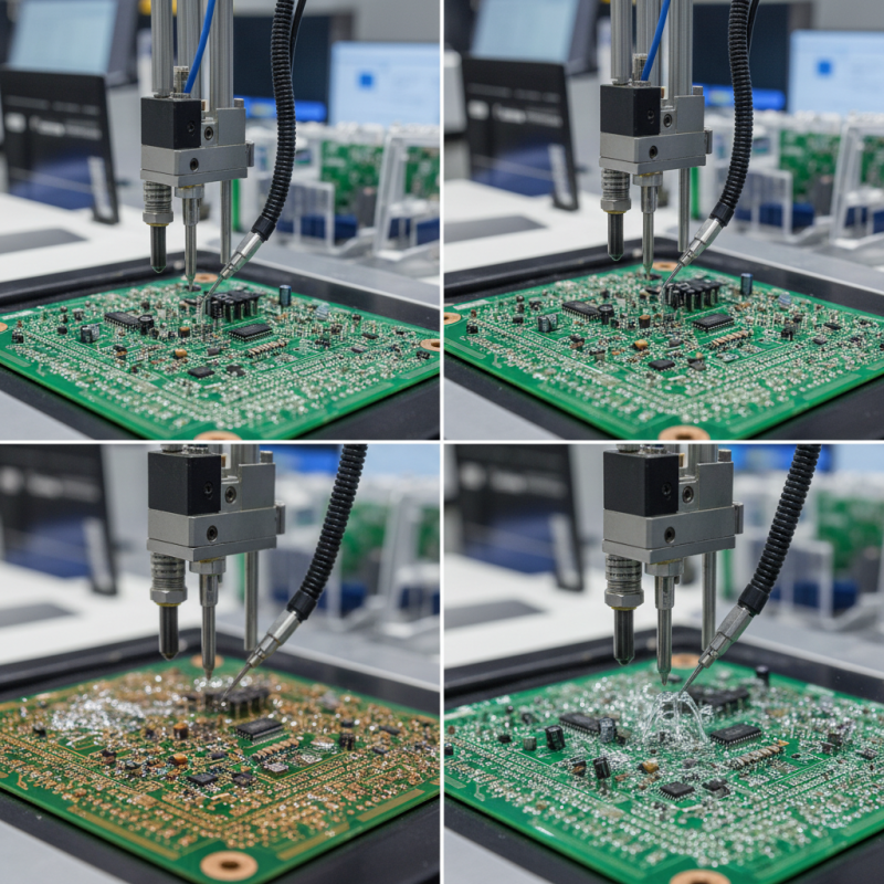
After the layers are prepared, they need to be etched. This is where the circuits are formed. The boards are exposed to chemicals. This step is critical. If not done correctly, the entire board may be ruined. Following etching, components are added. Soldering is done to fix them in place. At this stage, testing is also major. Every board is checked for faults. Missing a flaw can be costly.
PCB Manufacturing Process Overview
This bar chart illustrates the time spent on each step of the PCB manufacturing process. From design to final assembly, understanding the duration of each phase helps in optimizing production efficiency.
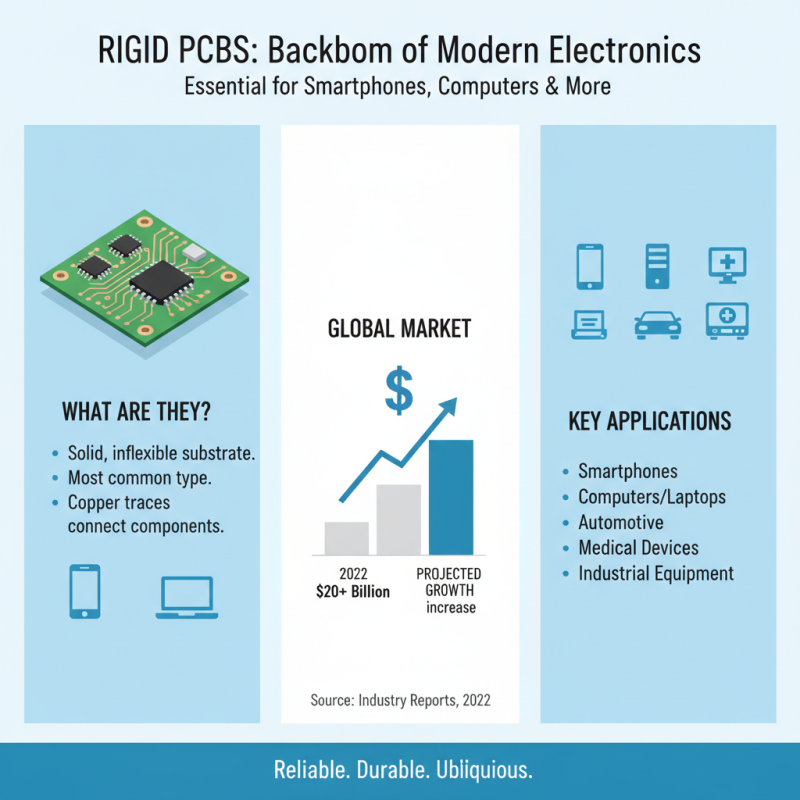
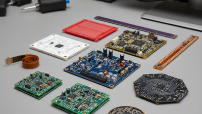
Types of PCBs and Their Applications
Printed Circuit Boards (PCBs) vary widely in type and application across numerous industries. Rigid PCBs are the most common, consisting of a solid substrate. They are essential for devices like smartphones and computers. According to industry reports, the global rigid PCB market was valued at over $20 billion in 2022, with significant growth projected in the upcoming years.
Flexible PCBs, on the other hand, offer unique advantages. They bend without breaking, making them ideal for wearable technology and compact devices. The flexibility also allows for innovative design solutions. Research indicates that the flexible PCB market may reach $16 billion by 2025, reflecting increasing demand in consumer electronics.
Another type is the multilayer PCB, which consists of multiple layers of circuitry. This design is crucial in high-density applications, such as medical equipment and aerospace technology. However, manufacturing these boards can be complex. The intricacy often leads to higher costs and longer lead times. It's essential to weigh these factors against performance needs. Each type of PCB serves a distinct purpose, but manufacturers must constantly adapt to technological advancements and market requirements. Failing to do so can lead to inefficiencies and lost opportunities.
Key Technologies and Equipment Used by PCB Makers
PCB makers rely on various key technologies and equipment to produce printed circuit boards. One essential tool is the photolithography machine. It transfers circuit patterns onto the PCB surface. This process is intricate and requires accuracy. Slight errors can lead to defective boards, which is a challenge for many makers.
Another crucial piece of equipment is the etching machine. It removes unwanted copper from the board. Precision is vital here, too. If not done correctly, you may end up with shorts or open circuits. Many PCB makers often struggle with achieving the exact specifications required for complex designs.
Lastly, solder mask application is critical. It protects the conductive traces on the board. This step can be tricky. Application flaws can lead to issues in soldering components. Over time, makers learn to refine their techniques. Each mistake teaches valuable lessons, highlighting the need for continuous improvement.