What is PCB Board Design? A Complete Guide for Beginners and Pros
The field of PCB board design has evolved significantly over the past few decades, driven by advancements in technology and the increasing demand for more complex electronic systems. According to a recent report by Research and Markets, the global PCB market is expected to reach USD 85.16 billion by 2027, growing at a CAGR of 4.4% from 2020 to 2027. This growth reflects the critical role that effective PCB board design plays in ensuring the functionality, reliability, and efficiency of electronic devices across various sectors, including consumer electronics, automotive, and telecommunications.
In addition to the financial growth, the complexity of PCB designs has also increased, necessitating a deep understanding of electronic principles, design software, and manufacturing processes. For beginners and seasoned professionals alike, mastering PCB board design is essential to navigate the challenges of modern electronics. Key considerations in the design process involve not only the layout and routing of traces but also aspects such as thermal management and signal integrity. As the technology landscape continues to shift towards higher frequencies and miniaturization, a solid grasp of PCB board design principles will remain paramount for success in the electronics industry.

Understanding the Basics of PCB Board Design
Understanding the basics of PCB board design is essential for both beginners and seasoned professionals in the electronics industry. Printed Circuit Boards (PCBs) serve as the backbone of most electronic devices, providing the physical platform for electrical components and enabling connectivity between them. According to a report by Research and Markets, the global PCB market is projected to reach $82 billion by 2026, reflecting the increasing demand for sophisticated electronic components in various sectors, including consumer electronics, automotive, and telecommunications.
At its core, PCB design involves several critical steps, such as schematic capture, layout design, and verification. Schematic capture allows designers to create a representation of the circuit, while layout design involves arranging components and traces on the board to ensure optimal performance. The IPC-2221 standard highlights key design guidelines, emphasizing the importance of minimizing trace lengths, optimizing component placement, and ensuring proper grounding to reduce signal interference. By adhering to these guidelines and utilizing software tools, designers can significantly enhance the reliability and manufacturability of PCBs.
Moreover, understanding materials and technology trends plays a crucial role in PCB design. For instance, the rise of flexible PCBs is driving innovation in various applications, as they allow for the development of lightweight and compact designs. As reported by IPC's "Flexible Circuits Market Report," the flexible circuit market is expected to grow at a compound annual growth rate (CAGR) of 6.5% through 2024. This shift not only represents a growing segment within the PCB industry but also emphasizes the need for designers to stay abreast of technological advancements to maintain competitive advantages.
Key Components of PCB Design: What You Need to Know
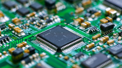
When embarking on PCB design, it's crucial to understand the key components that form the backbone of the board. At the heart of any PCB layout are the conductive pathways, typically made from copper, which facilitate electrical connections between various components. These traces must be designed with consideration for the current they will carry and the impedance they will introduce. Proper sizing and spacing are essential, as they not only impact performance but also influence factors such as heat dissipation and electromagnetic interference.
Another critical aspect of PCB design is the arrangement of components, including resistors, capacitors, and integrated circuits. Understanding their function within the circuit and the requirements for power distribution is paramount. It’s vital to consider factors like signal integrity and grounding, ensuring that the layout minimizes potential issues such as crosstalk and noise. Additionally, software tools for PCB design often include features for simulating electrical behavior, which can be invaluable for optimizing the layout before physical production, ensuring a robust and reliable final product.
What is PCB Board Design? A Complete Guide for Beginners and Pros - Key Components of PCB Design: What You Need to Know
| Component |
Description |
Material |
Common Uses |
| PCB Substrate |
The base material on which the circuit is built. |
FR-4, CEM-1 |
Consumer electronics, automotive |
| Copper Traces |
Conductive pathways that connect various components. |
Copper |
Signal transmission, power distribution |
| Solder Mask |
Protective layer that prevents solder from bridging between traces. |
Polymer |
Surface mount technology |
| Silkscreen Layer |
Layer used to add labels and logos to the PCB. |
Epoxy ink |
Component identification |
| Via |
Plated hole that allows connections between different layers. |
Copper |
Layer transitions |
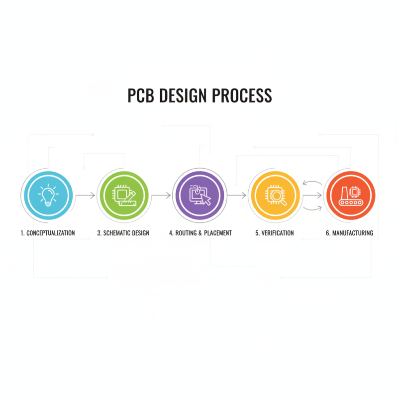
The Design Process: Step-by-Step Guide for PCB Creation
The design process for printed circuit boards (PCBs) is a systematic approach that involves several key steps, ensuring that the final product meets both functional and aesthetic requirements. The journey begins with conceptualization, where designers outline the intended functionality and overall layout of the PCB. This stage includes the creation of a schematic diagram that depicts the electrical connections and components. Accurate schematic design is crucial as it serves as the blueprint for the entire PCB layout.
Following the schematic phase, designers transition to the PCB layout stage. This involves placing components on the board and routing traces that connect them according to the schematic diagram. Attention to detail is critical at this point, as factors like trace width, clearance, and component placement can significantly impact the board’s performance and manufacturability. Designers often utilize specialized software to visualize the PCB and simulate electrical performance, ensuring that the design will function as intended before production.
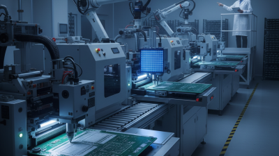
Once the layout is finalized, the next step is generating necessary files for manufacturing, including Gerber files that define the PCB layers and drill data. This documentation allows for accurate fabrication of the board. After production, the final phase includes testing and validation to confirm that the PCB performs according to specifications. Throughout the entire design process, effective communication and collaboration among team members are vital to address any issues that arise and to deliver a successful PCB that meets all design criteria.
Software Tools for PCB Design: Popular Options and Features
When it comes to PCB (Printed Circuit Board) design, choosing the right software tool is crucial for both beginners and experienced professionals. A recent industry report indicates that the global PCB design software market is projected to reach $1.5 billion by 2025, driven by the increasing demand for advanced electronics in various sectors, including automotive, telecommunications, and consumer electronics. As the complexity of electronics continues to rise, the need for robust software solutions becomes paramount.
Among the popular options for PCB design software, there are several key features that designers should consider. First, user-friendly interfaces and ease of learning are essential for beginners to create their first designs efficiently. Advanced simulation capabilities, including signal integrity and thermal management features, are crucial for experienced engineers to validate their designs before manufacturing. Additionally, robust collaboration tools that allow multiple users to work on the same project in real-time are increasingly popular, reflecting the growing trend towards remote work environments. According to recent studies, 75% of engineers report that collaborative tools enhance their productivity and lead to better design outcomes.
Another important functionality to look for in PCB design software is comprehensive libraries for components. With millions of electronic components available in the market, up-to-date libraries help designers save time and reduce errors. Data shows that approximately 30% of design time can be consumed by searching and verifying components, making an extensive and well-maintained library a significant asset in the design process. Overall, selecting the right PCB design software can significantly influence the efficiency and success of any electronics project, making it a critical consideration for all designers.
PCB Design Software Tools Popularity
Best Practices for Optimizing PCB Layout and Performance
Optimizing PCB layout and performance is crucial for designing efficient and effective circuit boards. One of the best practices is to strategically place components to minimize signal paths and reduce electromagnetic interference (EMI). Components that interact frequently should be positioned close together to limit the length of traces, thereby enhancing signal integrity and reducing noise. Furthermore, using ground planes and properly defining power distribution networks can significantly improve performance by ensuring stable voltage levels across the board.
When it comes to trace routing, keeping the traces as short and direct as possible is invaluable. This not only mitigates potential signal degradation but also simplifies the design, making it easier to troubleshoot. Implementing appropriate trace widths tailored to the current requirements will help prevent overheating and maintain performance efficiency.
**Tips:** Always consider the thermal management of your PCB; proper spacing can aid in heat dissipation, while copper pours can assist in spreading heat. Additionally, using vias wisely can help maintain a compact layout without sacrificing performance; express caution, though, as excessive vias can introduce unwanted inductance. Ultimately, balancing the mechanical and electrical aspects of PCB design will lead to a more reliable and functional product.