2025 How to Optimize PCB Layout for Better Performance and Efficiency
In the fast-evolving world of electronics, optimizing PCB layout is crucial for enhancing both performance and efficiency. As technology advances, the complexity of circuit designs increases, making effective PCB layout strategies more important than ever. Renowned PCB design expert, Dr. Emily Carter, emphasizes this necessity by stating, "A well-optimized PCB layout not only reduces signal integrity issues but also improves thermal management, paving the way for more reliable electronic systems."
This insight highlights the dual focus on performance metrics and efficiency gains that a skilled PCB layout can provide. As designers navigate the intricate balance between component placement, routing, and thermal considerations, the impact of their decisions on overall system performance becomes increasingly evident. With growing demands for compactness and functionality in electronic devices, the imperative to refine PCB layout techniques is clear.
In this article, we will explore effective strategies to optimize PCB layout for better performance and efficiency, delving into best practices and innovative approaches that can lead to superior designs. By understanding and implementing these techniques, designers can ensure their creations meet the rigorous standards of today's competitive market.
Understanding the Importance of PCB Layout Optimization
The optimization of PCB layout is crucial for enhancing both performance and efficiency in electronic devices. A well-designed PCB layout can significantly reduce electromagnetic interference (EMI), improve signal integrity, and minimize power loss. By carefully considering factors such as trace width, spacing, and component placement, engineers can ensure that the electrical paths are not only functional but also optimized for speed and stability. This is particularly vital in high-frequency applications where even minor inaccuracies in layout can lead to detrimental effects on the overall circuit performance.
Moreover, optimizing PCB layout extends the lifespan of electronic components and reduces the potential for overheating. By strategically placing heat-sensitive parts away from heat-generating ones and providing ample ground planes, designers can create a thermal management system that enhances reliability. Additionally, an efficient layout allows for more compact designs, which is increasingly important in consumer electronics where space is at a premium. Emphasizing layout optimization not only bolsters the immediate performance of the PCB but also leads to energy savings and longer operational life, ultimately aligning with the broader goals of sustainability in engineering practices.
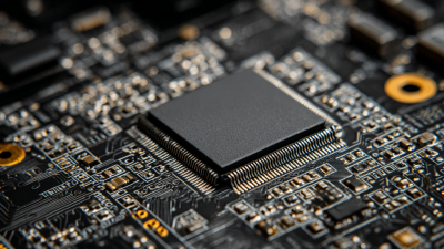
Key Principles of Effective PCB Design for Performance Enhancement
When optimizing PCB layouts for enhanced performance and efficiency, understanding the key principles of effective design is crucial. One primary principle is the importance of minimizing trace lengths. Shorter traces reduce inductance and capacitance, which can significantly decrease signal degradation and improve overall circuit performance. Additionally, maintaining proper spacing between traces helps prevent crosstalk, ensuring that signals remain clear and interference-free.
Tips for optimizing your PCB layout include conducting thorough signal integrity analysis to identify potential issues early in the design process. Utilizing a ground plane can also improve the return path for signals, leading to reduced noise and better overall performance. Another critical aspect is the strategic placement of components; ensuring that high-frequency devices are placed appropriately can enhance the efficiency of the circuit.
Lastly, thermal management should not be overlooked. Implementing adequate heatsinks and considering airflow in your layout can prevent overheating and enhance the long-term reliability of your PCB. By following these principles and tips, designers can create PCBs that not only function better but also maximize energy efficiency.
Performance and Efficiency Optimization in PCB Layout
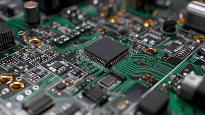
Techniques to Minimize Signal Interference in PCB Layout
Minimizing signal interference in PCB layout is a crucial aspect of optimizing performance and efficiency. According to a report by IPC, nearly 80% of PCB failures can be attributed to signal integrity issues, highlighting the importance of effective design techniques. One primary approach is the strategic placement of components. Keeping high-frequency components close together minimizes the length of the signal paths, reducing the potential for crosstalk and electromagnetic interference. This is supported by findings from the IEEE, which indicate that controlling the trace length can improve signal integrity by up to 30%.
Another effective technique is the implementation of ground planes. Utilizing a solid ground plane can act as a shield, helping to absorb and redirect unwanted noise away from sensitive areas of the PCB. The ESD Association reports that incorporating proper grounding techniques can reduce susceptibility to electrostatic discharge by more than 50%, further enhancing overall system reliability. Additionally, using differential pairs for signal lines helps cancel out noise, with industry studies suggesting that this technique can lead to improvements in signal-to-noise ratios by about 20%. Organizations looking to improve their PCB layouts should consider these techniques to ensure better operational efficiency and design longevity.
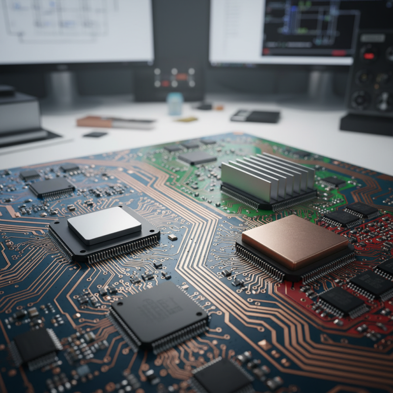
Best Practices for Thermal Management in PCB Design
The global PCB design market is poised for substantial growth, expanding from $257.2 million in 2023 to $926 million by 2030, driven by a compound annual growth rate of 20.1%. North America currently dominates this market, reflecting the region’s robust technology sector and innovation in PCB applications. As the demand for high-performance electronics rises, effective thermal management has become a critical focus in PCB layout optimization to enhance overall performance and efficiency.
Thermal management strategies are vital in PCB design, particularly when working with advanced materials like Gallium Nitride (GaN). GaN technology, known for its superior thermal efficiency and reduced parasitic capacitance compared to traditional silicon MOSFETs, necessitates meticulous layout practices to ensure adequate heat dissipation. Techniques such as proper component placement, thermal vias, and the use of thermal management materials can significantly mitigate overheating risks, leading to improved reliability and extended operational life of electronic devices. In an era of increasing electronic sophistication, implementing these best practices will be crucial for engineers looking to maximize the potential of their designs.
Utilizing Simulation Tools for Optimal PCB Layout Efficiency
In the design of printed circuit boards (PCBs), utilizing simulation tools has become essential for achieving optimal layout efficiency and performance. Recent industry reports indicate that rigorous simulation during the design phase can reduce time to market by up to 30%, allowing engineers to iterate their designs quickly without the need for multiple physical prototypes. By implementing tools such as finite element analysis (FEA) and electromagnetic simulation, designers can predict how components behave under various conditions, leading to more effective thermal management and signal integrity.
Moreover, simulation tools can help optimize the layout by providing insights into electromagnetic interference (EMI) and noise coupling between components. According to a 2023 report from IPC, 70% of design teams that incorporated simulation software saw a marked improvement in first-pass yield, reducing costly rework and enhancing overall efficiency. As the demand for compact and high-performance electronics increases, leveraging these advanced simulation techniques becomes critical in ensuring that PCB designs not only meet but exceed performance expectations.
2025 How to Optimize PCB Layout for Better Performance and Efficiency
| Parameter |
Value |
Impact on Performance |
Simulation Tool Used |
| Trace Width |
0.5 mm |
Reduces resistance, improves current carrying capacity |
Altium Designer |
| Layer Count |
6 Layers |
Enhanced signal integrity and reduced cross talk |
Eagle PCB |
| Via Type |
Blind Vias |
Lowers inductance, optimizes routing space |
KiCAD |
| Copper Weight |
1 oz/ft² |
Improves thermal management and durability |
Cadence OrCAD |
| Layout Density |
High Density |
Maximizes board space, allows for compact designs |
Mentor Graphics PADS |