What Is a PCB Manufacturer and How Can I Find One Near Me?
A printed circuit board manufacturer does more than etch copper onto fiberglass. It converts engineering files into a tested, repeatable electronic platform. Its work may include design-for-manufacturing review, material selection, fabrication, assembly, inspection, and delivery. When searching for “pcb manufacturers near me,” location is useful, but it should not be your only filter.
Happy Holden, a veteran PCB engineer and author of The Printed Circuit Handbook, describes the PCB as “the foundation of all electronic products.” That foundation must remain stable under heat, vibration, electrical stress, and production pressure. A capable manufacturer should explain its layer-count limits, minimum trace width, controlled-impedance process, surface finishes, and inspection methods. Ask for evidence, not broad promises. Certifications, sample reports, customer references, and clear tolerance data matter.
Nearby support can shorten shipping times and simplify design discussions. You might visit a facility, review a first article, or resolve a solder-mask issue across the table. However, distance alone can mislead. A local supplier may lack advanced HDI capability, while a farther manufacturer may offer stronger testing and better process control. I have also learned that the cheapest quotation can hide setup fees, material substitutions, or weak communication. That is an uncomfortable detail. It deserves attention.
This guide explains what PCB manufacturers actually do and how to compare “pcb manufacturers near me” with confidence. You will see which questions reveal technical competence, dependable quality, realistic lead times, and responsible production practices. Good sourcing is not guesswork. It is documented judgment.
What Does a PCB Manufacturer Do? From Gerber Files to Finished Boards
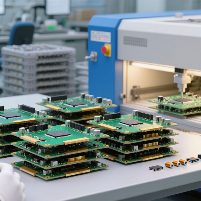
A PCB manufacturer turns design data into a tested circuit board. The process begins with Gerber files, drill files, and a bill of materials. These files define copper layers, holes, solder masks, and component locations. An experienced manufacturer checks them before production begins. This review can reveal missing apertures, unclear tolerances, or mismatched layer dimensions. Small errors matter. A single wrong drill size can delay assembly or weaken a connection.
After the design review, engineers choose suitable materials and board thicknesses. They then image copper patterns, drill holes, plate connections, and apply protective solder masks. Automated optical inspection checks the visible circuits. Electrical testing can identify open or short connections. During a prototype review, I would also inspect edge quality, silkscreen clarity, and connector fit. These details are easy to overlook. A reliable supplier should explain testing methods, production limits, and expected lead times clearly. Ask for sample inspection records and confirm how design changes are documented. Local manufacturers may offer easier communication, faster shipping, and visits to their facility. However, nearby does not always mean better. Compare certifications, engineering support, minimum order quantities, and quality-control procedures before choosing a partner.
Which PCB Specifications Matter? Layers, 1-oz (35-µm) Copper, and IPC Classes
A PCB manufacturer turns circuit designs into tested boards through imaging, etching, lamination, drilling, plating, and inspection. When searching near you, ask for process evidence, not only a low quote. The IPC 2024 PCB Technology Roadmap highlights higher density, finer features, and stronger reliability demands across electronics manufacturing. Your supplier should explain those limits clearly.
Layer count affects routing space, signal integrity, thickness, and cost. A two-layer board may suit a simple controller, while dense interfaces often need four or more layers. One-ounce copper means about 35 µm before processing. It does not automatically define finished thickness or current capacity. Trace width, temperature rise, plating, and thermal relief still matter. IPC-2221 provides design guidance, while IPC-6012 covers qualification requirements for rigid boards. IPC Class 2 suits general products; Class 3 demands tighter acceptance criteria for high-reliability equipment. Choose by consequence, not habit.
Tips: Send your fabricator the layer stackup, finished copper requirement, minimum trace and drill sizes, material type, and IPC class. Request a capability table and a sample inspection report. Ask how they verify inner-layer registration and plated-hole quality. A cheap board can become expensive after assembly. I have seen teams over-specify copper, then miss the real bottleneck: heat removal. Recheck the design with your manufacturer’s actual data. Mistakes hide in “standard” settings.
What Is a PCB Manufacturer and How Can I Find One Near Me?
Which PCB Specifications Matter? Layers, 1-oz (35-µm) Copper, and IPC Classes
Layers
Layer count describes the number of conductive copper layers. More layers can support denser routing, controlled impedance, and power distribution.
Copper Weight
A nominal 1-oz copper layer is approximately 35 µm thick. Heavier copper can carry more current but may require wider spacing and different manufacturing processes.
IPC Classes
IPC Class 1 targets general electronics, Class 2 supports dedicated-service products, and Class 3 is intended for high-reliability applications.
The chart shows commonly specified nominal copper weights and their approximate finished thicknesses. When comparing PCB manufacturers, confirm layer count, copper thickness, material requirements, tolerances, and the required IPC performance class.
How Can You Evaluate Suppliers? ISO 9001, IPC-A-600, and Class 3 Quality
A PCB manufacturer turns circuit designs into physical boards through imaging, etching, drilling, plating, and inspection. When searching for one near you, distance matters less than controlled production. A nearby supplier can support factory visits, sample reviews, and faster communication when problems appear.
ISO 9001
ISO 9001 shows that a supplier follows a documented quality management system. Ask how it controls design files, incoming materials, process changes, and corrective actions. Request recent audit findings, not only a certificate. Paperwork can look perfect.
IPC-A-600 gives visual and dimensional acceptance criteria for finished printed boards. Ask whether inspectors are trained to apply the standard consistently. Review sample reports for solderability, conductor spacing, hole quality, and surface defects.
Class 3 is intended for high-reliability applications, where failure may cause serious consequences. It demands tighter acceptance expectations than Class 1 or Class 2. However, Class 3 should match your product’s real risk, not serve as a marketing label.
Ask for the supplier’s inspection plan, electrical test coverage, material certificates, and lot traceability. Check whether test equipment is calibrated and whether failed boards are analyzed clearly.
A factory tour can reveal practical details, such as clean storage, labeled reels, and controlled humidity. I would also compare two or three local suppliers using the same questions.
My earlier mistake was trusting a polished presentation too quickly. Evidence from recent production is more useful than confident promises.
How Do You Find a PCB Manufacturer Near You? Compare MOQ, Lead Time, and Cost
A PCB manufacturer converts your circuit design into a physical printed circuit board. Finding one nearby can simplify communication, inspections, and shipping. Search regional directories, industrial parks, and engineering networks. Then contact several manufacturers with the same files.
Use Gerber files, a bill of materials, board thickness, layer count, and testing requirements. Ask each company to quote the same specification. Compare the minimum order quantity, or MOQ. A low MOQ suits prototypes, while a higher MOQ may reduce the unit price. Do not assume the cheapest board is the best choice.
Lead time needs careful checking. Ask whether it includes engineering review, fabrication, testing, and shipping. A quoted five-day build may become two weeks after approval. Get every milestone in writing. Cost also includes setup fees, tooling, shipping, inspection, and possible rework. Small details matter.
A reliable manufacturer should explain tolerances, material options, quality checks, and production capacity clearly. Request sample inspection reports or anonymized quality records when available. Visit the facility if practical. I once focused too heavily on unit price and overlooked delivery risk. That decision created scheduling pressure. My comparison now uses total landed cost, realistic lead time, and MOQ together. A local supplier is useful, but local does not automatically mean faster or more affordable. Ask difficult questions early.