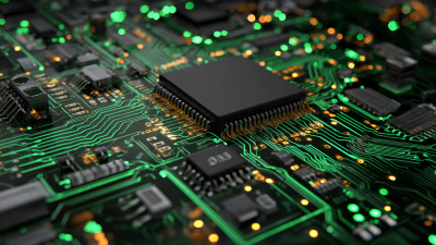
Top 5 Essential Features of High Quality PCB Boards for Your Projects
In the rapidly advancing world of electronics, the importance of high-quality PCB boards cannot be overstated. According to a recent market analysis by Mordor Intelligence, the global PCB market is expected to reach USD 89.6 billion by 2025, driven by the demand for innovative electronic devices across various sectors, including automotive, telecommunications, and consumer electronics. This surge illustrates the critical role that printed circuit boards play in the performance, reliability, and efficiency of modern electronic systems.
To achieve optimal performance in every project, it is essential to understand the key features that differentiate high-quality PCB boards from their lower-quality counterparts. A study conducted by ResearchAndMarkets highlights that enhanced thermal management, increased layer count, and improved surface finish are some of the paramount characteristics contributing to the overall effectiveness of PCBs. As engineers and developers strive to incorporate advanced technologies into their designs, knowing these essential features will not only streamline the manufacturing process but also ultimately enhance the longevity and functionality of the final product.
In this article, we will explore the top five essential features that define high-quality PCB boards, providing insights that can guide your projects toward successful outcomes. By understanding these characteristics, you will be better equipped to choose PCBs that align with your project requirements and ensure the reliability of your electronic applications.
Choosing the Right Materials for Durable PCB Boards
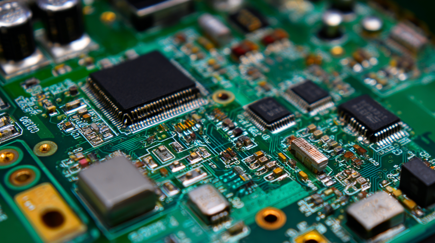
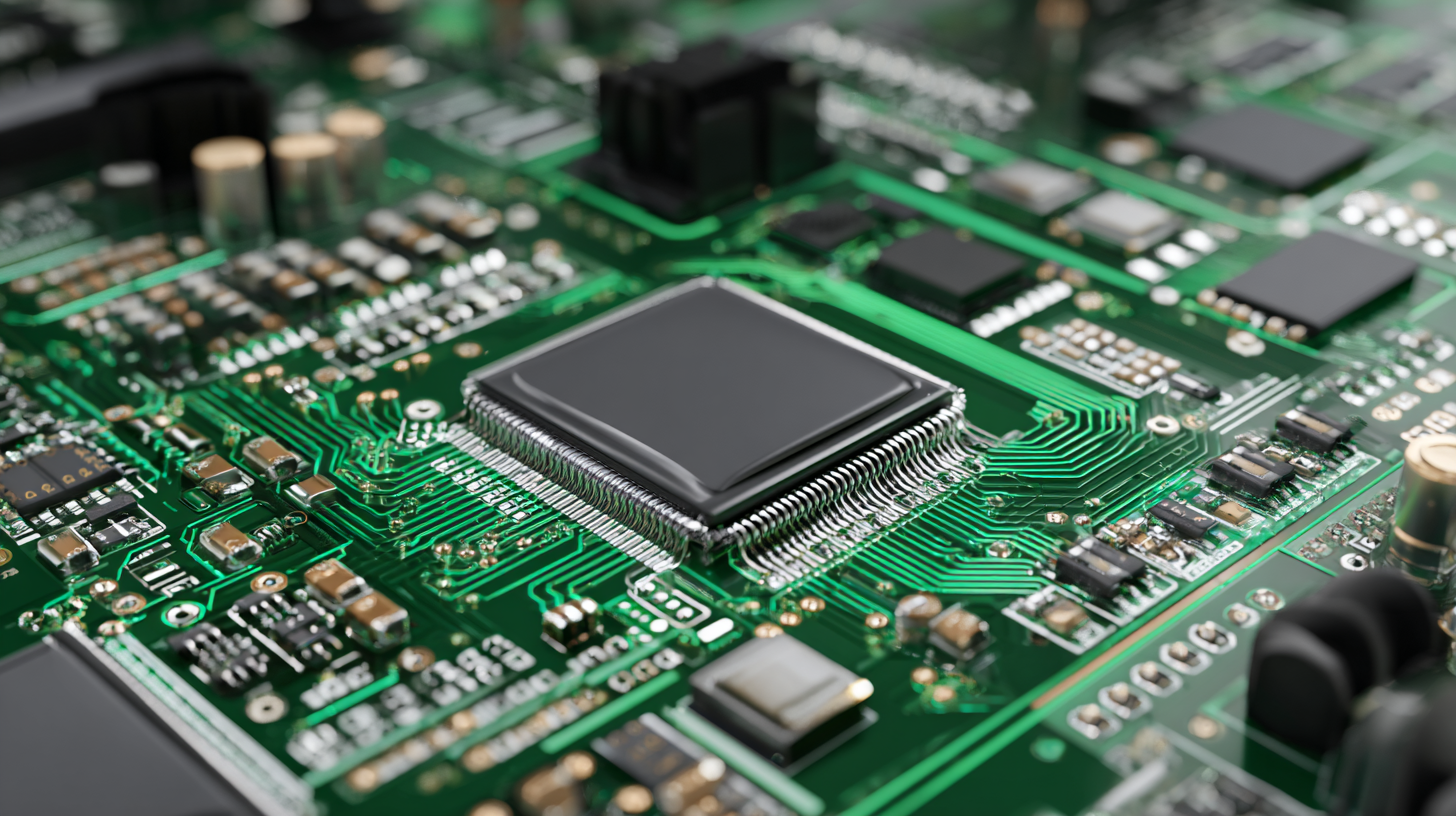
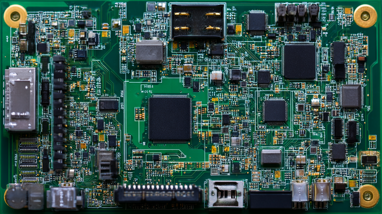
When selecting materials for durable PCB boards, the choice of substrate is paramount. One of the most commonly used materials is FR-4, a composite of woven glass fabric and epoxy resin. This material is favored for its excellent mechanical strength and resilience against temperature variations, making it ideal for a range of electronic applications.
 Additionally, advanced materials such as Rogers substrates offer superior thermal performance and lower dielectric losses, which is crucial for high-frequency applications.
Another critical factor in material selection is the copper plating thickness. Thicker copper layers lead to higher current-carrying capabilities and improved heat dissipation, which is essential for power supply circuits. Furthermore, surface finishes like ENIG (Electroless Nickel Immersion Gold) not only provide excellent solderability but also enhance the long-term reliability of PCB connections. By carefully choosing materials based on project specifications, engineers can ensure the longevity and performance of their electronic designs.
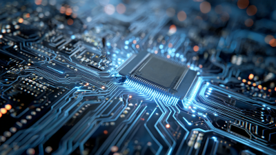
Understanding Layer Count and Its Impact on PCB Performance
When considering the design of high-quality PCB boards, layer count plays a crucial role in determining performance. PCBs typically come in single-layer, double-layer, or multi-layer configurations. Each additional layer contributes to enhanced functionality, allowing for more complex circuits and improved signal integrity. For projects that require high-speed data transmission or intricate designs, opting for a multi-layer PCB can greatly minimize electromagnetic interference and crosstalk.
Tip: When designing your PCB, analyze your project's needs carefully. If you're working with high-frequency applications, a four-layer or even an eight-layer PCB might be necessary to ensure optimal performance and reliability.
Moreover, the layer count affects not only performance but also manufacturing costs and timeframe. A higher number of layers can complicate the production process, increasing both time and cost. Therefore, it’s essential to strike the right balance between complexity and cost-effectiveness.
Tip: Consider prototyping with a lower layer count first to validate your design before committing to a more complex and expensive solution. This approach allows for adjustments based on practical observations while keeping costs manageable.
Importance of Trace Width and Spacing for Signal Integrity
When designing high-quality PCB boards, the importance of trace width and spacing cannot be overstated, especially for maintaining signal integrity in high-speed applications. According to recent studies, improper trace dimensions can lead to signal integrity issues, adversely impacting overall performance. For instance, inadequate spacing between traces can cause crosstalk, while insufficient trace width may result in increased resistance and heat generation, ultimately leading to circuit failure.
To optimize trace design, it is recommended to adhere to established high-speed design rules. The use of pre-layout simulation tools can assist engineers in visualizing potential issues before fabrication. One of the key insights from industry research suggests that employing scattering parameters in signal transmission analysis can provide a clearer understanding of how different designs will perform under various conditions.
Tips:
- Always consult design guidelines for trace width and spacing based on the specifications of your components to minimize potential signal degradation.
- Utilize advanced simulation tools to identify and correct issues early in the PCB design process, ensuring robust performance in critical applications.
- Implement differential signaling wherever possible, as it can help mitigate electromagnetic interference and enhance signal integrity in high-speed designs.
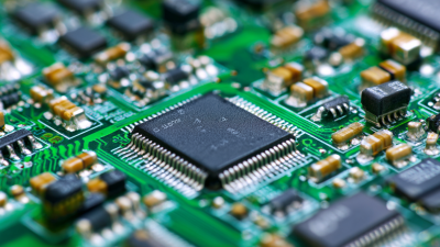
Evaluating Surface Finish Options for Enhanced PCB Longevity
When it comes to enhancing the longevity of printed circuit boards (PCBs), the surface finish option plays a crucial role. According to a report by IPC, around 80% of PCB failures can be attributed to surface issues, which underscores the importance of selecting an appropriate finish. Common surface finishes include Hot Air Solder Leveling (HASL), Electroless Nickel Immersion Gold (ENIG), and Organic Solderability Preservative (OSP). Each of these options presents its own advantages and considerations for long-term use.
ENIG, for example, has gained significant traction in the industry due to its excellent solderability and prolonged shelf life. Data from the International Electronics Manufacturing Initiative shows that ENIG finishes can extend PCB life cycles by up to 30%, making them an appealing choice for high-reliability applications. On the other hand, OSP provides a more environmentally friendly option as it does not involve hazardous materials, yet it may require more careful handling due to its susceptibility to moisture, which can significantly impact its performance over time. Careful evaluation of these surface finishes is essential to ensure optimal functionality and durability of PCBs in various projects.
Design Considerations for Enhanced Thermal Management in PCBs
In the realm of PCB design, thermal management is paramount, especially as electronic devices become increasingly compact and powerful. Effective thermal management ensures that components operate within their optimal temperature ranges, thereby enhancing efficiency and longevity. Various strategies can be employed, such as selecting materials with high thermal conductivity and designing layout configurations that allow for better heat dissipation.
Tips:
1. When designing, prioritize copper thickness. Increased copper thickness can significantly improve heat dissipation, making it a critical factor in high-current applications.
2. Incorporate thermal vias in your designs to facilitate heat transfer from hot components to the PCB substrate or a heat sink. This can drastically reduce the risk of overheating.
Innovation in PCB manufacturing has led to the adoption of advanced materials and designs that focus on thermal management. Multi-layer PCBs, which often utilize glass fiber, provide structural integrity while allowing sophisticated thermal pathways. Understanding and implementing these design considerations will elevate the performance of your electronic projects, particularly in demanding applications like electric vehicle charging systems.