How to Design an Effective PCB Layout for Your Projects?
A well-designed PCB layout is crucial for any electronics project. According to Dr. Emily Chen, an expert in PCB design, “A good layout can make or break your project.” Her insight highlights the importance of this often-overlooked stage in product development. Effective PCB layout minimizes interference and enhances performance.
When creating a PCB layout, it's essential to focus on component placement. Placing components logically can reduce trace lengths. This is often easier said than done, though. Many designers struggle with the balance between space and functionality. Additionally, keeping power and ground traces separate is critical for performance, yet it can complicate the design.
Reflecting on common pitfalls, designers often disregard thermal management. Overheating can damage components, yet it is frequently overlooked. Also, ignoring signal integrity can lead to unexpected failures. Striving for an effective PCB layout involves careful planning, testing, and, sometimes, redesigning. The journey can be challenging, but the rewards of a well-optimized design are invaluable.
Understanding PCB Layout Basics: Key Concepts for Design Success
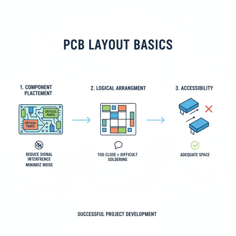
Understanding PCB layout basics is essential for successful project development. The foundation of a good layout starts with component placement. Components should be arranged logically. Critical parts need proximity to reduce signal interference. This helps in minimizing noise issues. Keep in mind that sometimes we overlook the importance of accessibility. Placing components too close can make soldering difficult.
Routing traces is another key concept. Wider traces can handle more current. It’s often tempting to use narrow paths for a clean look. But that can lead to overheating and failures. Ground planes should be larger than necessary to provide a solid reference. However, many designs underestimate the importance of ground integrity.
Design rules, like keeping trace lengths short, can be easily ignored. Long traces might look neat but can affect signal speed. Similarly, using vias can complicate layouts. They add inductance and resistance, which can affect performance. Reflect on these choices carefully during the design process. Remember, a few mistakes can lead to major issues down the line.
Identifying Design Requirements: Schematic and Component Selection
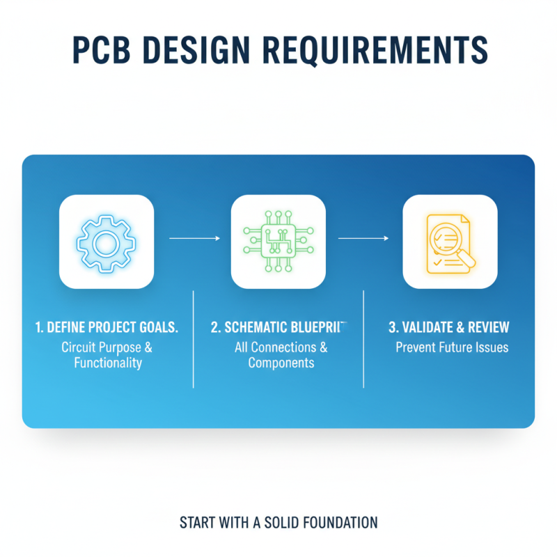
Identifying design requirements is a critical first step in creating an effective PCB layout. Start by outlining the project goals clearly. Know what your circuit should accomplish, whether it’s for a simple gadget or a complex device. The schematic serves as your blueprint. Ensure it reflects all connections and functionalities. Missing connections can lead to issues later on.
Next, consider component selection. Choose parts based on availability and specifications. Keep in mind the voltage, current ratings, and sizes. Components must fit together well on the board. Sometimes, the ideal part may not be available. You may need to reconsider your design. Be ready to adapt your schematic based on component choices. This flexibility can enhance your final layout but might also lead to a few unanticipated challenges.
Document everything. Notes on component behavior and connection requirements will assist during layout. Stay organized; however, it’s not uncommon to overlook some details. Make revisions as necessary. Reflecting on your choices can aid in developing a more efficient design process. Analyze what works and what doesn’t to refine your approach in future projects.
Utilizing Design Software Tools: Features for PCB Layout Optimization
Designing an effective PCB layout is crucial for the success of any electronic project. Using design software tools can significantly enhance this process. These tools often provide features that allow for real-time error checking. They can highlight potential mistakes before you even start the manufacturing process. This saves time and resources.
Many design software options offer intuitive interfaces. They allow users to visualize the board layout with ease. Layer management features help you organize different components effectively. Components can be placed with precision. However, it’s easy to overlook some details. Sometimes, the connections may seem okay but lead to short circuits later on. Pay attention to trace routing; it should be logical and straightforward.
The software's simulation capabilities are also worth mentioning. They allow you to test how your design performs under different conditions. This can reveal issues that you might miss if relying solely on visual checks. Still, not all tool features are easy to grasp. Some require a learning curve or come with hidden complexities. This can lead to confusion if you rush through your design. It's important to embrace the imperfections in your initial layouts. They are learning opportunities for improvement.
How to Design an Effective PCB Layout for Your Projects?
| Design Software Tool |
Key Features |
Advantages |
Typical Use Cases |
| Eagle |
Schematic capture, PCB layout, library management |
User-friendly interface, extensive library |
Small to medium projects, hobbyist designs |
| KiCAD |
Open-source, schematic editing, 3D viewer |
Free to use, actively developed |
Academic projects, prototyping |
| Altium Designer |
Unified design platform, advanced routing tools |
Powerful for complex designs, high productivity |
Professional and large-scale projects |
| OrCAD |
Schematic capture, PCB routing, simulation |
Robust design tools, high-level analysis |
Automotive and industrial designs |
| EasyEDA |
Online platform, collaborative design, order PCBs |
Accessible from anywhere, community support |
Startups, educational purposes |
Implementing Best Practices: Trace Routing and Ground Plane Design
When designing a PCB layout, trace routing is crucial for performance. According to a report by IPC, improper routing can lead to up to 30% signal loss. Proper trace width can improve conductivity and reduce heat. The IPC Standard recommends a width of at least 0.5 mm for current-carrying traces. This ensures safe operation without excessive voltage drop.
Ground plane design is equally important. A solid ground plane minimizes electromagnetic interference (EMI). A study by IEEE indicates that well-designed ground planes can reduce EMI by 40%. However, many designers overlook potential ground loops. These loops can introduce noise, affecting signal integrity. It’s vital to maintain short, direct paths to the ground plane to avoid this issue.
Bending traces can introduce parasitic capacitance, complicating signal integrity. A common mistake is not considering the return path for high-frequency signals. High-speed designs may require careful planning to manage return paths effectively. Think about adding vias for optimal routing. This can enhance layout efficiency, but it also demands more attention to detail.
Testing and Validation: Ensuring Functional Integrity of the PCB Layout
Testing and validating a PCB layout is crucial for ensuring its functional integrity. Designing a PCB is only part of the process. After laying out the components, testing begins. This is where real-world conditions come into play. You might think you’ve created a flawless design, but problems can arise unexpectedly.
Functional tests should cover all aspects. Power distribution is critical. Simulate various operating conditions to find weaknesses. Inspect signal integrity as well. Use an oscilloscope to track down any irregularities. However, the results can reveal that your layout isn’t as effective as you hoped. Did you place components in a way that minimizes interference?
Reflect on the results. Did you overlook thermal management? Heat can cause failures, and you may need to redesign the layout. Interactivity between nearby components could also lead to issues. Identify these flaws and make necessary adjustments. Testing isn’t just a final step; it’s a learning process. Each error identified enhances your design skills.
PCB Layout Test Results 2023