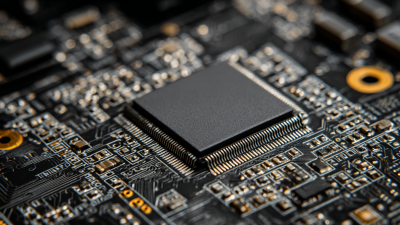
2026 Best PCB Printing Techniques for Improved Circuit Board Design?
In the fast-evolving world of electronics, PCB printing plays a crucial role in circuit board design. According to a recent report from market research firm MarketsandMarkets, the PCB printing market is projected to reach $78 billion by 2026. This growth highlights the increasing demand for innovative techniques in PCB manufacturing.
Expert Dr. Emily Chen, a leading authority in the field, states, "The future of PCB printing lies in our ability to enhance precision and efficiency." Yet, achieving this goal is not without challenges. Current techniques can be inconsistent, leading to defects that compromise circuit reliability. This underscores the need for continuous improvement in methodologies and technology.
As the industry evolves, designers must remain vigilant. They should address both the opportunities and limitations of current PCB printing practices. The path to superior circuit board design requires an ongoing commitment to innovation and quality assurance. Embracing new techniques will inevitably transform how we approach PCB printing today and in the future.
Overview of PCB Printing Techniques for Circuit Board Design
Advancements in PCB printing techniques are crucial for modern circuit board design. The industry is witnessing a shift toward more efficient manufacturing processes. Reports indicate that 72% of companies are adopting advanced printing technologies to enhance performance. These techniques promise higher precision and reduced waste, yet challenges remain.
One prominent method is additive manufacturing, known for its flexibility. It enables the creation of complex geometries. However, precision can be a concern. Maintaining consistency across large production volumes often proves difficult. Research shows that 65% of engineers find post-processing issues common when using this technique. They report a need for better quality control.
Another technique gaining traction is screen printing. This method is favored for its cost-effectiveness. Yet, it can fall short in fine detail resolution. A notable 58% of manufacturers cite this limitation as a barrier. Addressing these imperfections is key for future innovation. Emerging technologies could bridge these gaps, but it requires industry-wide collaboration.
Traditional vs. Modern Printing Techniques Used in PCB Manufacturing
In the world of PCB manufacturing, traditional methods like screen printing and etching are widely known. Screen printing uses stencils to apply conductive ink onto substrates. This process has remained popular for years due to its cost-effectiveness and ease of use. However, traditional techniques often face limitations. For example, achieving fine lines can be challenging. Errors in alignment occur often, leading to wasted materials.
Modern printing techniques, such as inkjet and laser printing, are gaining traction. These methods allow for greater precision. For instance, inkjet technology can produce intricate designs that were once impossible. Moreover, laser printing offers a faster way to create prototypes. This efficiency can significantly shorten development cycles. Yet, there are hurdles to overcome. Equipment costs can be high, and learning curves may deter new users.
It’s essential to reflect on these methods' advantages and disadvantages. Traditional techniques can produce reliable results, but they may not keep pace with growing demands for complexity. On the other hand, modern methods promise innovation, but the initial investment can be risky. Balancing cost, speed, and quality remains a crucial challenge in PCB manufacturing.
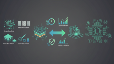
Key Factors Influencing PCB Quality and Performance
When designing a printed circuit board (PCB), several factors can significantly affect both quality and performance. Material choice is vital. Using high-grade substrates improves conductivity, durability, and reliability. However, not all materials are suitable for every application. Sometimes, cost constraints push engineers to opt for less effective options, which may lead to failures in the long run.
Another crucial element is the layout and design of the PCB. Proper spacing between traces prevents short circuits. Designers should consider the thickness of traces as well. Thinner traces can be susceptible to damage from heat. In some cases, it may be tempting to cram components into a small space. This can create issues like signal interference and overheating. It's a balancing act that requires attention to detail.
Finally, manufacturing techniques play a role. Techniques like laser etching offer precision, but they can be more costly. Many firms wonder if they should invest in advanced methods or stick with traditional approaches that may not always yield the best results. Each technique has its pros and cons. Errors during production can mar even the best initial designs. A constant reevaluation of processes is essential.
2026 Best PCB Printing Techniques for Improved Circuit Board Design
| Printing Technique |
Key Features |
Advantages |
Disadvantages |
Applications |
| Screen Printing |
Uses a mesh to transfer ink onto the substrate. |
High throughput; suitable for large runs. |
Less detail for fine features; slower than other methods. |
Suitable for basic circuit designs. |
| Inkjet Printing |
Sprays tiny droplets of ink on the substrate. |
High precision; capable of multi-layer printing. |
Higher cost of equipment; slower speed. |
Prototyping and small series production. |
| Laser Direct Imaging (LDI) |
Uses lasers to expose photoresist on the PCB. |
Great for fine features; eliminates photomasks. |
Requires advanced setup; higher initial costs. |
High-density applications and complex designs. |
| Electroplating |
Deposits a metal layer through an electrochemical process. |
Strong and reliable connections. |
Complex setup; requires careful handling. |
High-performance and high-reliability circuits. |
| Pad Printing |
Uses a silicone pad to transfer ink from a plate to the substrate. |
Versatile and good for irregular surfaces. |
Limited resolution; slower than other methods. |
Applications requiring designs on curved surfaces. |
Innovative Materials and Technology in PCB Printing
The evolution of PCB printing techniques continues to shape circuit board design. Innovative materials play a crucial role. Advanced inks, such as conductive polymers, enhance electrical performance. These materials allow for finer features and greater design flexibility. They can also reduce the weight and thickness of boards. Yet, challenges remain.
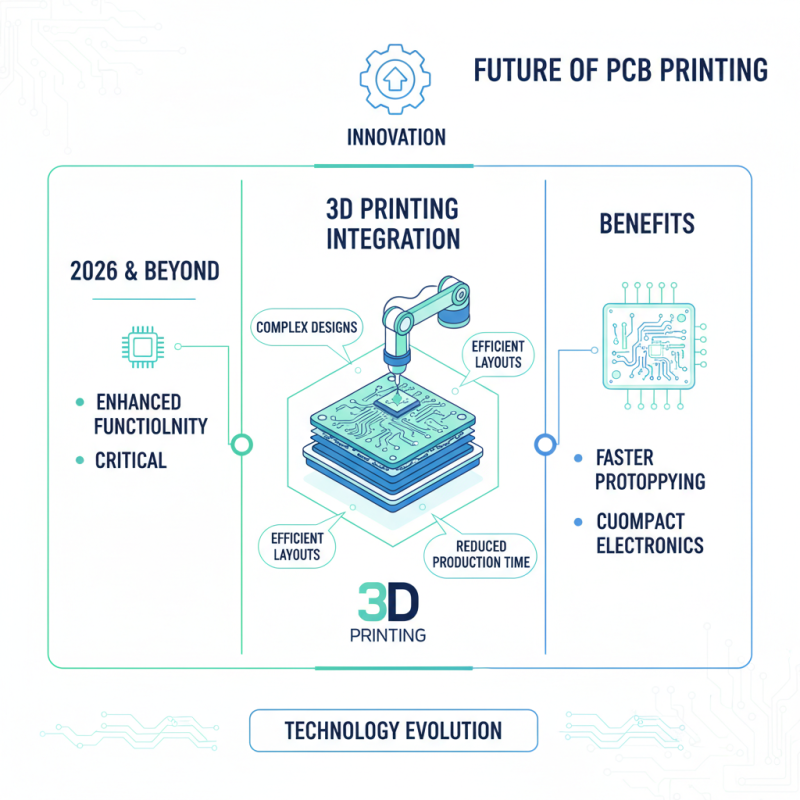
Despite the benefits, not all materials are reliable. Some conductive inks may degrade over time. This leads to potential failures in circuits. It's vital for designers to test these materials thoroughly. The integration of new technologies like 3D printing adds another layer of complexity. While it allows for unique designs, it can also result in inconsistencies. Ensuring quality and durability is paramount.
Another exciting area is the use of eco-friendly materials. While they align with sustainable practices, some still lack performance comparison to traditional options. Designers need to weigh these factors carefully. Balancing innovation and reliability is key to advancing PCB design. Exploration is essential, but accountability is equally important.
2026 Best PCB Printing Techniques for Improved Circuit Board Design
The chart below showcases the various PCB printing techniques based on their adoption rate in 2026. These techniques are essential for optimizing circuit board design, enhancing performance and reliability.