
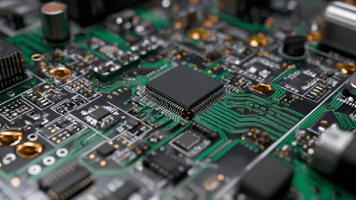
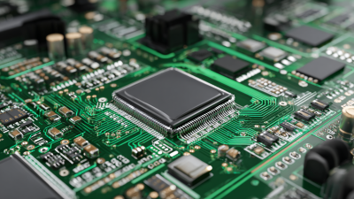
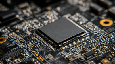
10 Best Circuit Board Design Tools for Efficient Electronics Development
In the fast-evolving realm of electronics development, the significance of effective circuit board design cannot be overstated. According to a recent report by MarketsandMarkets, the global circuit board design software market is projected to reach USD 2.89 billion by 2025, highlighting the critical role that robust design tools play in driving innovation and efficiency in this sector. As technology continues to advance, the tools used for circuit board design are becoming increasingly sophisticated, enabling engineers to create more complex and reliable electronic systems.
Renowned circuit board design expert Dr. Elaine Johnson emphasizes the importance of choosing the right design tools, stating, "The efficiency of the design process directly correlates with the quality of the end product. Innovative circuit board design tools are essential for reducing errors and enhancing productivity." This sentiment reflects the industry's understanding that a well-designed circuit board not only improves device performance but also accelerates time-to-market for new electronic products.
As we explore the 10 best circuit board design tools available today, it is important to recognize that these tools not only aid in the mechanical layout of components but also facilitate collaboration among multidisciplinary teams. With the advent of advanced simulation and verification capabilities, engineers are empowered to push the boundaries of what is possible in circuit board design, ultimately leading to more cutting-edge electronic solutions.

Top 5 Features to Look for in Circuit Board Design Tools for Enhanced Productivity

When selecting circuit board design tools, several key features can significantly enhance productivity and efficiency in electronics development. First and foremost, an intuitive user interface is crucial. A clean, organized layout allows designers to navigate the software easily, reducing the learning curve and facilitating quick project setup. Features like drag-and-drop functionality can streamline the design process, enabling designers to focus more on creativity rather than technicalities.
Another important feature is collaboration support. In today’s development landscape, team projects are common, so tools that allow real-time collaboration can make a significant difference. This includes cloud integration, version control, and communication features that ensure all team members are on the same page. Additionally, robust simulation capabilities are essential. A tool that provides accurate predictions and simulations of electrical performance can save time by identifying potential issues before physical prototypes are created. Overall, prioritizing these features can lead to a smoother design process and improved end results in circuit board projects.

Related Posts
-

2025 Top 5 Trends in Circuit Board Design You Can't Afford to Miss
-

The Future of Printed Circuit Boards: Innovations Shaping Our Electronic Devices
-

Top 10 Tips for Efficient Circuit Board Manufacturing Process Optimization
-
The Future of Electronics Innovating with PCB Design Software for Beginners
-
Top 5 Essential Features of High Quality PCB Boards for Your Projects
-
Unlocking Efficiency: The Future of PCB Production Techniques in Modern Electronics